| Edit Values | |
| Zen 2 µarch | |
| General Info | |
| Arch Type | CPU |
| Designer | AMD |
| Manufacturer | TSMC |
| Introduction | 2019 |
| Process | 7 nm |
| Succession | |
Zen 2 is a planned microarchitecture being developed by AMD as a successor to Zen+. Zen 2 is expected to be succeeded by Zen 3.
Contents
History
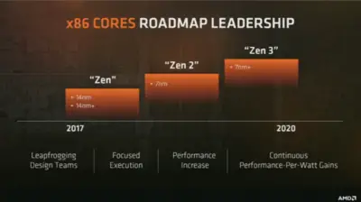
Zen 2 is set to succeed Zen in the future, sometimes around 2019. In February of 2017 Lisa Su, AMD's CEO announced their future roadmap to include Zen 2 and later Zen 3. On Investor's Day May 2017 Jim Anderson, AMD Senior Vice President, confirmed that Zen 2 is set to utilize 7 nm process.
Codenames
| Core | C/T | Target |
|---|---|---|
| Rome | Up to 64/128 | High-end server multiprocessors |
| Castle Peak | ?/? | workstation & enthusiasts market processors |
| Matisse | ?/? | Mainstream to high-end desktops & enthusiasts market processors |
| Picasso | ?/? | Mainstream desktop & mobile processors with GPU |
Process technology
Zen 2 is fabricated on TSMC's 7 nm process.
Compiler support
| Compiler | Arch-Specific | Arch-Favorable |
|---|---|---|
| GCC | -march=znver2 |
-mtune=znver2
|
- Note: Initial support in GCC 9.
Architecture
Zen 2 inherits most of the design from Zen+ but improves the instruction stream bandwidth and floating-point throughput performance.
Key changes from Zen+
- 7 nm process (from 12 nm)
- I/O die still utilizes 14 nm
- Core
- Front-end
- Improved branch prediction unit
- Improved prefetcher
- Improved µOP cache tags
- Improved µOP cache
- Larger µOP cache (?? enters, up from 2048)
- Increased dispatch bandwidth
- Improved branch prediction unit
- Back-end
- Increased retire bandwidth (??-wide, up from 8-wide)
- FPU
- 2x wider datapath (256-bit, up from 128-bit)
- 2x wider EUs (256-bit FMAs, up from 128-bit FMAs)
- 2x wider LSU (2x256-bit L/S, up from 128-bit)
- Front-end
- Security
- In-silicon Spectre enhancements
- Increase number of keys/VMs supported
- I/O
- PCIe 4.0 (from 3.0)
- Infinity Fabric 2
- 2.3x transfer rate per link (25 GT/s, up from ~10.6 GT/s)
This list is incomplete; you can help by expanding it.
New instructions
Zen 2 introduced a number of new x86 instructions:
-
CLWB- Force cache line write-back without flush -
RDPID- Read Processor ID -
WBNOINVD- Force cache line write-back without invalidation
Block Diagram
Individual Core
| This section is empty; you can help add the missing info by editing this page. |
Memory Hierarchy
| This section is empty; you can help add the missing info by editing this page. |
Core
Zen 2 largely builds on Zen. Most of the fine details have not been revealed by AMD yet.
Front End
In order to feed the backend, which has been widened to support 256-bit operation, the front-end throughput was improved. AMD reported that the branch prediction unit has been reworked. This includes improvements to the prefetcher and various undisclosed optimizations to the instruction cache. The µOP cache was also tweaked including changes to the µOP cache tags and the µOP cache itself which has been enlarged to improve the instruction stream throughput.
Execution Engine
AMD stated that both the dispatch bandwidth and the retire bandwidth has been increased.
Floating Point
The floating-point unit underwent major modifications in Zen 2. In Zen, AVX2 256 bit single and double precision vector floating-point data types were supported through the use of two 128 bit micro-ops per instruction. Likewise, the floating-point load and store operations were 128 bits wide. In Zen 2, the datapath and the execution units were widened to 256 bits, doubling the vector throughput of the core.
With two 256-bit FMAs, Zen 2 is capable of 16 FLOPs/cycle.
Bibliography
- AMD 'Tech Day', February 22, 2017
- AMD 2017 Financial Analyst Day, May 16, 2017
- AMD GCC 9 znver2 enablement patch
- AMD 'Next Horizon', November 6, 2018
See Also
- Intel Ice Lake
| codename | Zen 2 + |
| designer | AMD + |
| first launched | 2019 + |
| full page name | amd/microarchitectures/zen 2 + |
| instance of | microarchitecture + |
| manufacturer | TSMC + |
| microarchitecture type | CPU + |
| name | Zen 2 + |
| process | 7 nm (0.007 μm, 7.0e-6 mm) + |

