| Edit Values | |
| Gen9.5 µarch | |
| General Info | |
| Arch Type | GPU |
| Designer | Intel |
| Manufacturer | Intel |
| Introduction | August 30, 2016 |
| Process | 14 nm |
| Succession | |
Gen9.5 (Generation 9.5) is the microarchitecture for Intel's graphics processing unit utilized by Kaby Lake-based, Coffee Lake-based, and Goldmont Plus-based microprocessors. Gen9.5 is the successor to Gen9 used by Skylake and introduces a number of light enhancements.
Contents
Codenames
Various models support different Graphics Tiers (GT) which provides different levels of performance. Some models also support an additional eDRAM side cache.
| Code Name | Description |
|---|---|
| GT1 | Contains 1 slice with 12 execution units. |
| GT2 | Contains 1 slice with 24 execution units. |
| GT3 | Contains 2 slices with 48 execution units. |
| GT3e | Contains 2 slices with 48 execution units. Has an additional eDRAM side cache. |
| Halo (GT4e) | Contains 3 slices with 72 execution units. Has an additional eDRAM side cache. |
Models
| Gen9.5 IGP Models | Standards | ||||||||||||
|---|---|---|---|---|---|---|---|---|---|---|---|---|---|
| Name | Execution Units | Tier | Series | eDRAM | Vulkan | Direct3D | OpenGL | OpenCL | |||||
| Windows | Linux | Windows | Linux | HLSL | Windows | Linux | Windows | Linux | |||||
| UHD Graphics 600 | 12 | GT1 | Gemini Lake | - | 1.0 | 12 | N/A | 5.1 | 4.5 | 4.5 | 2.1 | 2.0 | |
| UHD Graphics 605 | 18 | GT1.5 | Gemini Lake | - | |||||||||
| HD Graphics 610 | 12 | GT1 | S, U | - | |||||||||
| HD Graphics 615 | 24 | GT2 | Y | - | |||||||||
| HD Graphics 620 | 24 | GT2 | U | - | |||||||||
| HD Graphics 630 | 24 | GT2 | S, H | - | |||||||||
| UHD Graphics 630 | 23/24 | GT2 | S | - | |||||||||
| HD Graphics P630 | 24 | GT2 | H | - | |||||||||
| Iris Plus Graphics 640 | 48 | GT3e | U | 64 MiB | |||||||||
| Iris Plus Graphics 650 | 48 | GT3e | U | 64 MiB | |||||||||
| Model | SKU | EUs | CPU Stepping[devID 1] | GT Stepping[devID 2] | Device2 ID[devID 3] | GT Device2 ID Revision[devID 4] |
|---|---|---|---|---|---|---|
| HD Graphics 610 | KBL DT 2+1F | 12 | 0x5902 | |||
| KBL U - ULT 2+1F | 0x5906 | |||||
| HD Graphics 615 | KBL Y - ULX 2+2 | 24 | 0x591E | |||
| HD Graphics 620 | KBL-U 2+2 | H0 | C0/B0 | 0x5916 | 0x2 | |
| HD Graphics 630 | KBL-S 4+2 | B0 | F0/C0 | 0x5912 | 0x4 | |
| KBL Halo 4+2 | 0x591B | |||||
| UHD Graphics 630 | CFL-S 4+2 | 23/24 | U0 | 0x3E91 | ||
| CFL-S 6+2 | U0 | 0x3E92 | ||||
| HD Graphics P630 | KBL WKS 4+2 | 24 | 0x591D | |||
| Iris Plus Graphics 640 | KBL-U 2+3 | 48 | J1 | D1/B1 | 0x5926 | 0x6 |
| Iris Plus Graphics 650 | KBL U - ULT 2+3E (28W) | 0x5927 |
- ↑ The CPU Stepping is the actual CPU design stepping.
- ↑ The GT Stepping refers to the GT design stepping.
- ↑ The Device2 ID is the PCI device ID that identifies the GT SKU for driver software
- ↑ The GT Device2 Revision ID identifies the silicon stepping for driver software.
Performance
| Frequency | Peak Performance | |||||||||||
|---|---|---|---|---|---|---|---|---|---|---|---|---|
| Half Precision | Single Precision | Double Precision | ||||||||||
| Models | 610 | 615, 620, 630, P630 | 640, 650 | 610 | 615, 620, 630, P630 | 640, 650 | 610 | 615, 620, 630, P630 | 640, 650 | |||
| Tiers | GT1 | GT2 | GT3e | GT1 | GT2 | GT3e | GT1 | GT2 | GT3e | |||
| Ref (FLOP/clk) | 384/cycle | 768/cycle | 1536/cycle | 192/cycle | 384/cycle | 768/cycle | 48/cycle | 96/cycle | 192/cycle | |||
| Base (300 MHz) | 115.2 GFLOPS | 230.4 GFLOPS | 460.8 GFLOPS | 57.6 GFLOPS | 115.2 GFLOPS | 230.4 GFLOPS | 14.4 GFLOPS | 28.8 GFLOPS | 38.7 GFLOPS | |||
| Base (350 MHz) | 134.4 GFLOPS | 268.8 GFLOPS | 537.6 GFLOPS | 67.2 GFLOPS | 134.4 GFLOPS | 268.8 GFLOPS | 16.8 GFLOPS | 33.6 GFLOPS | 45.15 GFLOPS | |||
| Boost (850 MHz) | 326.4 GFLOPS | 652.8 GFLOPS | 1,305.6 GFLOPS | 163.2 GFLOPS | 326.4 GFLOPS | 652.8 GFLOPS | 40.8 GFLOPS | 81.6 GFLOPS | 109.65 GFLOPS | |||
| Boost (900 MHz) | 345.6 GFLOPS | 691.2 GFLOPS | 1,382.4 GFLOPS | 172.8 GFLOPS | 345.6 GFLOPS | 691.2 GFLOPS | 43.2 GFLOPS | 86.4 GFLOPS | 116.1 GFLOPS | |||
| Boost (950 MHz) | 364.8 GFLOPS | 729.6 GFLOPS | 1,459.2 GFLOPS | 182.4 GFLOPS | 364.8 GFLOPS | 729.6 GFLOPS | 45.6 GFLOPS | 91.2 GFLOPS | 122.55 GFLOPS | |||
| Boost (1,000 MHz) | 384 GFLOPS | 768 GFLOPS | 1,536 GFLOPS | 192 GFLOPS | 384 GFLOPS | 768 GFLOPS | 48 GFLOPS | 96 GFLOPS | 129 GFLOPS | |||
| Boost (1,050 MHz) | 403.2 GFLOPS | 806.4 GFLOPS | 1,612.8 GFLOPS | 201.6 GFLOPS | 403.2 GFLOPS | 806.4 GFLOPS | 50.4 GFLOPS | 100.8 GFLOPS | 135.45 GFLOPS | |||
| Boost (1,100 MHz) | 422.4 GFLOPS | 844.8 GFLOPS | 1,689.6 GFLOPS | 211.2 GFLOPS | 422.4 GFLOPS | 844.8 GFLOPS | 52.8 GFLOPS | 105.6 GFLOPS | 141.9 GFLOPS | |||
| Boost (1,150 MHz) | 441.6 GFLOPS | 883.2 GFLOPS | 1,766.4 GFLOPS | 220.8 GFLOPS | 441.6 GFLOPS | 883.2 GFLOPS | 55.2 GFLOPS | 110.4 GFLOPS | 148.35 GFLOPS | |||
Hardware Accelerated Video
| [Edit] Kaby Lake (Gen9.5) Hardware Accelerated Video Capabilities | |||||||
|---|---|---|---|---|---|---|---|
| Codec | Encode | Decode | |||||
| Profiles | Levels | Max Resolution | Profiles | Levels | Max Resolution | ||
| MPEG-2 (H.262) | Main | High | 1080p (FHD) | Main | Main, High | 1080p (FHD) | |
| MPEG-4 AVC (H.264) | High, Main | 5.1 | 2160p (4K) | Main, High, MVC, Stereo | 5.1 | 2160p (4K) | |
| JPEG/MJPEG | Baseline | - | 16k x 16k | Baseline | Unified | 16k x 16k | |
| HEVC (H.265) | Main, Main 10 | 5.1 | 2160p (4K) | Main, Main 10 | 5.1 | 2160p (4K) | |
| VC-1 | ✘ | Advanced, Main, Simple | 3, High, Simple | 3840x3840 | |||
| VP8 | Unified | Unified | N/A | 0 | Unified | 1080p | |
| VP9 | 0 | 2160p (4K) | 0, 2 | Unified | 2160p (4K) | ||
Process Technology
- Main article: Kaby Lake § Process Technology
Gen9.5 are part of the Kaby Lake SoC die which uses an enhanced 14nm+ process.
Architecture
Gen9.5 is very similar to Gen9 with a number of enhancements.
Key changes from Gen9
- Enhanced "14nm+" process (while CPU cores base frequency was increased, GPU speed remains unchanged)
- Power consumption is reduced
- Display block
- Embedded DisplayPort (eDP) now supports eDP Standard 1.4 (From 1.3)
- Unslice
- New native hardware support for 4K HEVC/VP9
- WiDi (miracast) support has been enhanced
- VQE wider color gamma
- DRM
- Support for Microsoft's PlayReady 3.0
- HDCP 2.2
Block Diagram
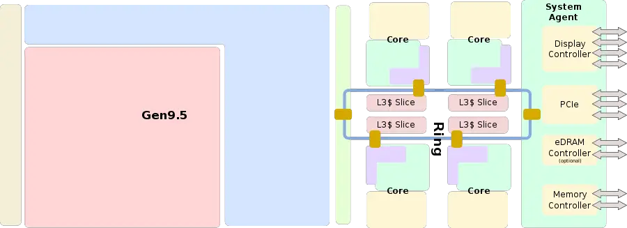
Entire SoC Overview
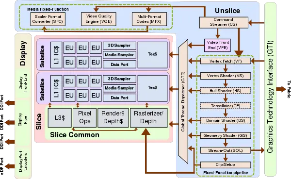
Gen9.5
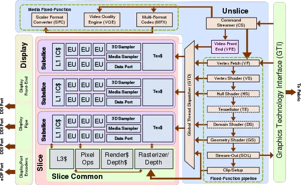
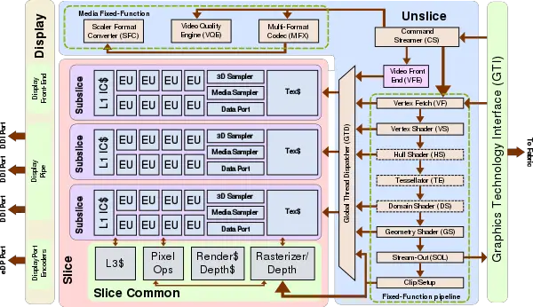
This block is for the most common setup, which is GT2 with 24 execution units.
Individual Core
See Kaby Lake#Individual_Core.
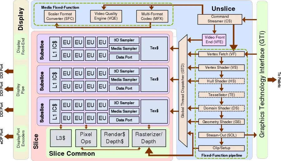
Unslice
The Unslice is one of the major components and is responsible for the fixed-function geometry capabilities, fixed-function media capabilities, and it provides the interface to the memory fabric. One of the big changes in Gen9 was that the Unslice now sits on its own power/clock domain. This change allows the Unslice to operate at its own speed provided higher on-demand performance when desired. This change has a number of other benefits such as being able to turn off the slices (one or more) when they're not used in cases where pure fixed-function media is used. Additionally, the Unslice is now capable of running at a higher clock while the slice can run at a slower clock when the scenario demands it (such as in cases where higher fixed-function geometry or memory demands occur).
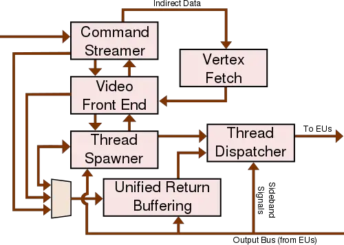
The Command Stream (CS) unit manages the the flow of execution for the FF Pipeline (3D Pipeline) and the Media pipelines. The CS unit performs the switching between pipelines and forwarding command streams to the different stages. Data in the pipeline are passed to the next unit using a messaging network. Messages can be passed directly through registers or by using the URB. The Command Stream also manages the allocation of the URB and supports the Constant URB Entry (CURB) function. The Unified Return Buffer (URB) is globally shared and is explicitly addressed. The pipeline's fixed-function blocks have both read and write access to the URB, additionally the shader cores have write access to the URB.
The media general-purpose pipeline consists of two fixed-function units: Video Front End (VFE) and the Thread Spawner (TS). The VFE unit handles the interfacing with the Command Streamer, writes thread payload data into the Unified Return Buffer, as well as prepares threads to be dispatched through TS unit. The VFE unit also contains the hardware Variable Length Decode (VLD) engine for MPEG-2 video decode. The TS unit is primarily responsible for interfacing with the Thread Dispatcher (TD) unit which is responsible for spawning new root-node parent threads originated from VFE unit and for spawning child threads (either leaf-node child threads or branch-node parent thread).
Fixed-Function
- Multi-Format Codec (MFX)
- HEVC Decode
- Support for HEVC & VP8 in PAK (for encode)
- New fixed function within MFX for real-time AVC encoding usages
- Video Quality Engine (VQE)
- 16-bit processing path
- 5x5 spatial denoise filter
- Local Adaptive Contrast Enhancement (LACE)
- Camera processing features to allow high-resolution raw camera processing
- Scalar and Format Conversion (SFC)
- Allows for inline format conversion & upscaling or downscaling of imagest
- Can be coupled with decoder to allow high-quality video processing in the FF units in the unslice without utilizing the media sampler in the slices themselves.
3D Pipeline Stages
| Pipeline Stage | Functions Performed |
|---|---|
| Command Stream (CS) | The Command Stream stage is responsible for managing the 3D pipeline and passing commands down the pipeline. In addition, the CS unit reads “constant data” from memory
buffers and places it in the URB. Note that the CS stage is shared between the 3D, GPGPU and Media pipelines. |
| Vertex Fetch (VF) | The Vertex Fetch stage, in response to 3D Primitive Processing commands, is responsible for reading vertex data from memory, reformatting it, and writing the results into Vertex URB Entries. It then outputs primitives by passing references to the VUEs down the pipeline. |
| Vertex Shader (VS) | The Vertex Shader stage is responsible for processing (shading) incoming vertices by passing them to VS threads. |
| Hull Shader (HS) | The Hull Shader is responsible for processing (shading) incoming patch primitives as part of the tessellation process. |
| Tessellation Engine (TE) | The Tessellation Engine is responsible for using tessellation factors (computed in the HS stage) to tessellate U,V parametric domains into domain point topologies.
Domain Shader (DS) The Domain Shader stage is responsible for processing (shading) the domain points (generated by the TE stage) into corresponding vertices. |
| Geometry Shader (GS) | The Geometry Shader stage is responsible for processing incoming objects by passing each object’s vertices to a GS thread. |
| Stream Output Logic (SOL) | The Stream Output Logic is responsible for outputting incoming object vertices into Stream Out Buffers in memory. |
| Clipper (CLIP) | The Clipper stage performs Clip Tests on incoming objects and clips objects if required. Objects are clipped using fixed-function hardware |
| Strip/Fan (SF) | The Strip/Fan stage performs object setup. Object setup uses fixed-function hardware. |
| Windower/Masker (WM) | The Windower/Masker performs object rasterization and determines visibility coverage |
Slice
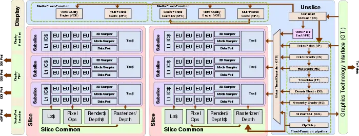
Slices are a cluster of subslices. For most configurations in Gen9.5, 3 subslices are aggregated into 1 slice to form a total of 24 execution units (depending on the model, some low end models do have less). The slice incorporates the thread dispatch routine, level 3 cache (L3$), a highly banked shared local memory structure, fixed function logic for atomics and barriers, and a number of fixed-function units for various media capabilities. The Global Thread Dispatcher (GTD) is responsible for load balancing thread distribution across the entire device. The global thread dispatcher works in concert with local thread dispatchers in each subslice.
Execution Unit (EU)
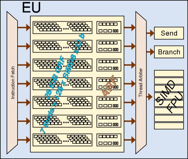
The Execution Units (EUs) are the programmable shader units - each one is an independent computational unit used for execution of 3D shaders, media, and GPGPU kernels. Internally, each unit is hardware multi-threaded capable of executing multi-issue SIMD operations. Execution is multi-issue per clock to pipelines capable of integer, single and double precision floating point operations, SIMD branch capability, logical operations, transcendental operations, and other miscellaneous operations. Communication between the EUs and the support units (shared function units such as operations involving texture sampling or scatter/gather load/stores) is done via messages that were programmatically constructed. Dependency hardware allows threads to sleep until the requested data is returned from those units.
Shared Functions are hardware units that provide a set of specialized supplemental functionality for the EUs. As their name implies they implement functions with insufficient demand to justify the cost of being implemented in the individual EUs. Functionality in these units are shared among the EUs in the subslice. Communication between the EUs and the Shared Function is done via lightweight message passing. Messages are a small self-contained packet of information created by a kernel and directed to a specific shared function. EU threads awaiting the return of a message from the Shared Function unit go into temporary sleep.
The Execution Unit is composed of 7 threads. Each thread has 128 SIMD-8 32-bit registers in a General-Purpose Register File (GRF) and supporting architecture specific registers (ARF). The EU can co-issue to four instruction processing units, including two FPUs, a branch unit, and a message send unit.
Preemption Granularity
Preemption in Gen9 (Skylake) was improved over Gen8 in a number of way. Preemption is important for multi-tasking system and especially important for improving responsiveness of operations (i.e. the ability to stop and start operations quickly with minimal latency interruption for the end user). In Broadwell (Gen8) Intel added support for the ability to stop operations on object-level for 3D workloads such as on a triangle boundary (i.e. beginning of a triangle, between two triangles, between two lines or points) and be able to preempt and restore back to those operations. In Gen9 Intel added the ability to stop execution units on an instruction boundary and be able to restore them (previously such preemption was only possible at the boundary of a kernel - i.e. the entire kernel execution must take places before preemption was possible). Gen9 added support for thread-group (complete kernel execution) to mid-thread (instruction boundary) for compute workloads:
Example of responsiveness (Source: IDF15)
| Application | Thread-Group Preemption | Mid-Thread Preemption | ||
|---|---|---|---|---|
| U Series | Y Series | U Series | Y Series | |
| Adobe Photoshop | 4-6 ms | 17-22 ms | 300 µs | 800 µs |
| Sample App1 | 200-500 ms | 200-500 ms | 300 µs | 280-320 µs |
| Sample App2 | 17 ms | 24 ms | 240 µs | 200-430 µs |
Display
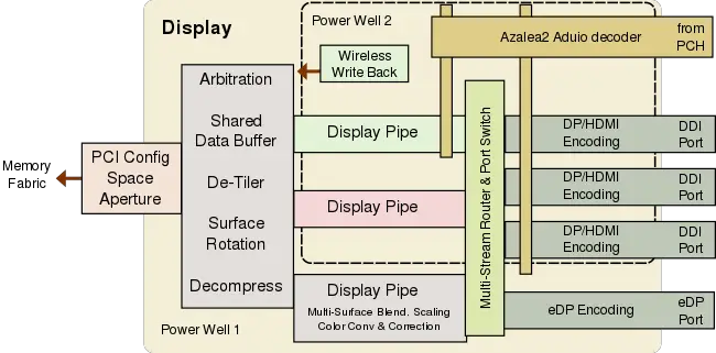
The display has a memory interface (supporting high memory bandwidth coming directly to the display sub-system), a front-end that is responsible for sorting and sequencing the requests (as well as handling things such as rotated displays), and display pipes. The display pipes perform input format conversion, multi-plane composition, color conversion, and scaling the result. The final part of the display port are the prot encoders that convert the input form the display pipes to the appropriate standard used (DP/HDMI/eDP). A number of improvements in Gen9 in the display block were done with respect to the display pipes, specifically being able to consume lossless compression directly without doing any extra unnecessary conversion operations. Additionally the pipes now support render compressed surfaces, Y-tiled surfaces, and on the fly 90/207 rotations.
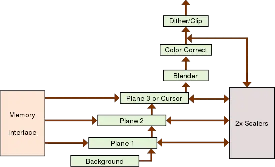
Multiple Display Planes in a Pipe
- Three plane sources + background
- All 3 are independent
- Fixed order (highest priority is plane3, lowest is background)
- Planes can be:
- YUV video
- RGB windows/desktop
- Fixed visual priority/blending order
- Color correction of result
- Two 7x5 scalers
- Bind to individual planes or pipe output
- Intended to support various OS features such as
- Microsoft's MPO (Multiplane overlay support)
- Android's SurfaceFlinger
Scalability
Gen9.5 can scale from 1 to 3 slices producing SKUs ranging from 12 to 72 execution units (note that the 12 EUs are formed from half a slice effectively).
GT1 (ULP)
GT1 is the most compact configuration offering two benefits: reduced cost and reduced power. GT1 is made of 1 slice containing 2 subslices with 6 EUs/subslice for a total of 12 EUs. With the scale-down, GT1 changes the ratio to 6:1 EU:sampler ratio. Note that this does retains the same ratio of 12 texels/clock and 8 pixels/clock at the backend. This configuration is better suited for some of the low power workload (e.g. ASTC-LDR+HDR, ETC1/2 compression). Note that software stack remains unchanged compared to the larger models.
GT1.5
GT1.5, offers 3 subslices of 6 EUs each for a total of 18 EUs.
GT2
GT2 is the standard configuration consisting of 1 slice with 3 subslices and 8 EU/subslice for a total of 24 EUs.
GT3
GT3 consists of 2 slices with 3 subslices in each and 8 EU/subslice for a total of 48 EUs.
Halo (GT4)
Codename Halo (GT4) is the most complex configuration offering the highest execution units count. Halo incorporates 3 slices with 3 subslices/slice and 8 EU/subslice for a total of 72 EUs.
Configuration
| Configuration Attribute (Source: Intel's Programmer's Ref Manual) | ||||||
|---|---|---|---|---|---|---|
| Attribute | Model | |||||
| GT1F (1x2x6) |
GT1.5F (1x3x6) |
GT2 (1x3x8) |
GT3 (2x3x8) | |||
| Global Attributes | ||||||
| Slice count | 1 | 1 | 1 | 2 | ||
| Subslice Count | 2 | 3 | 3 | 6 | ||
| EU/Subslice | 6 | 6 | 8 | 8 | ||
| EU count (total) | 12 | 18 | 24 | 48 | ||
| Thread Count | 7 | 7 | 7 | 7 | ||
| Thread Count (Total) | 84 | 126 | 161 / 168 | 329 / 336 | ||
| FLOPs/Clk - Half Precision, MAD (peak) | 384 | 576 | 736 / 768 | 1504 / 1536 | ||
| FLOPs/Clk - Single Precision, MAD (peak) | 192 | 288 | 368 / 384 | 752 / 768 | ||
| FLOPs/Clk - Double Precision, MAD (peak) | 48 | 72 | 92 / 96 | 188 / 192 | ||
| Unslice clocking (coupled/decoupled from Cr slice) | coupled | coupled | coupled | coupled | ||
| GTI / Ring Interfaces | 1 | 1 | 1 | 1 | ||
| GTI bandwidth (bytes/unslice-clk) | 64: R 64: W |
64: R 64: W |
64: R 64: W |
64: R 64: W | ||
| eDRAM Support | N/A | N/A | N/A | 0, 64 MiB | ||
| Graphics Virtual Address Range | 48 bit | 48 bit | 48 bit | 48 bit | ||
| Graphics Physical Address Range | 39 bit | 39 bit | 39 bit | 39 bit | ||
| Caches & Dedicated Memories | ||||||
| L3 Cache, total size (bytes) | 384K | 768K | 768K | 1536K | ||
| L3 Cache, bank count | 2 | 4 | 4 | 8 | ||
| L3 Cache, bandwidth (bytes/clk) | 2x 64: R 2x 64: W | 4x 64: R 4x 64: W | 4x 64: R 4x 64: W | 8x 64: R 8x 64: W | ||
| L3 Cache, D$ Size (Kbytes) | 192K - 256K | 512K | 512K | 1024K | ||
| URB Size (kbytes) | 128K - 192K | 384K | 384K | 768K | ||
| SLM Size (kbytes) | 0, 128K | 0, 192K | 0, 192K | 0, 384K | ||
| LLC/L4 size (bytes) | ~2MiB/CPU core | ~2MiB/CPU core | ~2MiB/CPU core | ~2MiB/CPU core | ||
| Instruction Cache (IC, bytes) | 2x 48K | 3x 48K | 3x 48K | 6x 48K | ||
| Color Cache (RCC, bytes) | 24K | 24K | 24K | 2x 24K | ||
| MSC Cache (MSC, bytes) | 16K | 16K | 16K | 2x 16K | ||
| HiZ Cache (HZC, bytes) | 12K | 12K | 12K | 2x 12K | ||
| Z Cache (RCZ, bytes) | 32K | 32K | 32K | 2x 32K | ||
| Stencil Cache (STC, bytes) | 8K | 8K | 8K | 2x 8K | ||
| Instruction Issue Rates | ||||||
| FMAD, SP (ops/EU/clk) | 8 | 8 | 8 | 8 | ||
| FMUL, SP (ops/EU/clk) | 8 | 8 | 8 | 8 | ||
| FADD, SP (ops/EU/clk) | 8 | 8 | 8 | 8 | ||
| MIN,MAX, SP (ops/EU/clk) | 8 | 8 | 8 | 8 | ||
| CMP, SP (ops/EU/clk) | 8 | 8 | 8 | 8 | ||
| INV, SP (ops/EU/clk) | 2 | 2 | 2 | 2 | ||
| SQRT, SP (ops/EU/clk) | 2 | 2 | 2 | 2 | ||
| RSQRT, SP (ops/EU/clk) | 2 | 2 | 2 | 2 | ||
| LOG, SP (ops/EU/clk) | 2 | 2 | 2 | 2 | ||
| EXP, SP (ops/EU/clk) | 2 | 2 | 2 | 2 | ||
| POW, SP (ops/EU/clk) | 1 | 1 | 1 | 1 | ||
| IDIV, SP (ops/EU/clk) | 1-6 | 1-6 | 1-6 | 1-6 | ||
| TRIG, SP (ops/EU/clk) | 2 | 2 | 2 | 2 | ||
| FDIV, SP (ops/EU/clk) | 1 | 1 | 1 | 1 | ||
| Load/Store | ||||||
| Data Ports (HDC) | 2 | 3 | 3 | 6 | ||
| L3 Load/Store (dwords/clk) | 2x 64 | 3x 64 | 3x 64 | 6x 64 | ||
| SLM Load/Store (dwords/clk) | 2x 64 | 3x 64 | 3x 64 | 6x 64 | ||
| Atomic Inc, 32b - sequential addresses (dwords/clk) | 2x 64 | 3x 64 | 3x 64 | 6x 64 | ||
| Atomic Inc, 32b - same address (dwords/clk) | 2x 4 | 3x 4 | 3x 4 | 6x 4 | ||
| Atomic CmpWr, 32b - sequential addresses (dwords/clk) | 2x 32 | 3x 32 | 3x 32 | 6x 32 | ||
| Atomic CmpWr, 32b - same address (dwords/clk) | 2x 4 | 3x 4 | 3x 4 | 6x 4 | ||
| 3D Attributes | ||||||
| Geometry pipes | 1 | 1 | 1 | 1 | ||
| Samplers (3D) | 2 | 3 | 3 | 6 | ||
| Texel Rate, point, 32b (tex/clk) | 8 | 12 | 12 | 24 | ||
| Texel Rate, point, 64b (tex/clk) | 8 | 12 | 12 | 24 | ||
| Texel Rate, point, 128b (tex/clk) | 8 | 12 | 12 | 24 | ||
| Texel Rate, bilinear, 32b (tex/clk) | 8 | 12 | 12 | 24 | ||
| Texel Rate, bilinear, 64b (tex/clk) | 8 | 12 | 12 | 24 | ||
| Texel Rate, bilinear, 128b (tex/clk) | 2 | 3 | 3 | 6 | ||
| Texel Rate, trilinear, 32b (tex/clk) | 8 | 12 | 12 | 24 | ||
| Texel Rate, trilinear, 64b (tex/clk) | 4 | 6 | 6 | 12 | ||
| Texel Rate, trilinear, 128b (tex/clk) | 1 | 1.5 | 1.5 | 3 | ||
| Texel Rate, aniso 2x, MIP Linear,, 32b (tex/clk) | 2 | 3 | 3 | 6 | ||
| Texel Rate, aniso 4x, MIP Linear,, 32b (tex/clk) | 1 | 1.5 | 1.5 | 3 | ||
| Texel Rate, ansio 8x, MIP Linear,, 32b (tex/clk) | 0.5 | 0.75 | 0.75 | 1.5 | ||
| Texel Rate, ansio 16x, MIP Linear,, 32b (tex/clk) | 0.25 | 0.375 | 0.375 | 0.75 | ||
| HiZ Rate, (ppc) | 64 | 64 | 64 | 2x 64 | ||
| IZ Rate, (ppc) | 16 | 16 | 16 | 2x 16 | ||
| Stencil Rate (ppc) | 64 | 64 | 64 | 2x 64 | ||
| Media Attributes | ||||||
| Samplers (media) | 2 | 3 | 3 | 6 | ||
| VDBox Instances | 1 | 1 | 1 | 2 | ||
| VEBox Instances | 1 | 1 | 1 | 2 | ||
| SFC Instances | 1 | 1 | 1 | 1 | ||
| Display Attributes | ||||||
| Display Pipes | 3 | 3 | 3 | 3 | ||
| Display Planes per Pipe | 3 | 3 | 3 | 3 | ||
| DDI ports | 2 | 2 | 2 | 2 | ||
| eDP ports | 1 | 1 | 1 | 1 | ||
Datasheets
Programmer's Reference Manual
- Volume 1: Preface
- Volume 2a: Command Reference: Instructions (Command Opcodes)
- Volume 2b: Command Reference: Enumerations
- Volume 2c: Command Reference: Registers Part 1 – Registers A through L
- Volume 2c: Command Reference: Registers Part 2 – Registers M through Z
- Volume 2d: Command Reference: Structures
- Volume 3: GPU Overview
- Volume 4: Configurations
- Volume 5: Memory Views
- Volume 6: Command Stream Programming
- Volume 7: 3D-Media-GPGPU
- Volume 8: Media VDBOX
- Volume 9: Media Video Enhancement (VEBOX) Engine
- Volume 10: HEVC Codec Pipeline (HCP)
- Volume 11: Blitter
- Volume 12: Display
- Volume 13: Memory-mapped Input/Output (MMIO)
- Volume 14: Observability
- Volume 15: Scaler Format Converter (SFC)
- Volume 16: Workarounds
| codename | Gen9.5 + |
| designer | Intel + |
| first launched | August 30, 2016 + |
| full page name | intel/microarchitectures/gen9.5 + |
| instance of | microarchitecture + |
| manufacturer | Intel + |
| microarchitecture type | GPU + |
| name | Gen9.5 + |
| process | 14 nm (0.014 μm, 1.4e-5 mm) + |
