Semiconductor & Computer Engineering
From WikiChip
Difference between revisions of "intel/microarchitectures/netburst (client)"
(→Willamette) |
(additional info for 1M and 2M L2) |
||
| Line 45: | Line 45: | ||
* {{intel|Prescott|l=core}} core | * {{intel|Prescott|l=core}} core | ||
* [[90 nm process]] | * [[90 nm process]] | ||
| − | * 135 mm² die size | + | * 1M L2 112 mm², 2M L2 135 mm² die size |
| − | * 169,000,000 transistors | + | * 125M, 169,000,000 transistors |
| − | + | 1M L2 | |
| − | |||
:[[File:netburst prescott core die.png|700px]] | :[[File:netburst prescott core die.png|700px]] | ||
| + | 2M L2 | ||
| + | :[[File:Pentium_4_6xx-die_2M.jpg|700px]] | ||
=== Additional Shots === | === Additional Shots === | ||
Revision as of 10:51, 26 August 2018
| Edit Values | |
| NetBurst µarch | |
| General Info | |
| Arch Type | CPU |
| Designer | Intel |
| Manufacturer | Intel |
| Introduction | November 20, 2000 |
| Phase-out | April, 2006 |
| Process | 180 nm |
| Instructions | |
| ISA | x86-32, x86-64 |
| Succession | |
NetBurst (also P68) was the microarchitecture for Intel's 180 nm process for desktops and servers as a successor to P6. NetBurst was replaced by the Core microarchitecture in early 2006.
Die
Willamette

- Willamette core
- 180 nm process
- 217 mm² die size
- 42,000,000 transistors

Northwood
- Northwood core
- 130 nm process
- 131 mm² die size
- 55,000,000 transistors

Prescott
- Prescott core
- 90 nm process
- 1M L2 112 mm², 2M L2 135 mm² die size
- 125M, 169,000,000 transistors
1M L2

2M L2

Additional Shots
Additional die and wafer shots provided by Intel:
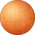
Netburst wafer

Facts about "NetBurst - Microarchitectures - Intel"
| codename | NetBurst + |
| designer | Intel + |
| first launched | November 20, 2000 + |
| full page name | intel/microarchitectures/netburst (client) + |
| instance of | microarchitecture + |
| instruction set architecture | x86-32 + and x86-64 + |
| manufacturer | Intel + |
| microarchitecture type | CPU + |
| name | NetBurst + |
| phase-out | April 2006 + |
| process | 180 nm (0.18 μm, 1.8e-4 mm) + |