(→NVLink 2.0) |
(→NVLink 2.0) |
||
| Line 75: | Line 75: | ||
== NVLink 2.0 == | == NVLink 2.0 == | ||
NVLink 2.0 was first introduced with the {{nvidia|V100}} [[GPGPU]] based on the {{nvidia|Volta|l=arch}} microarchitecture along with [[IBM]]'s {{ibm|POWER9|l=arch}}. Nvidia added CPU mastering support, allowing both the GPU and CPU to access each others memory (i.e., direct load and stores) in a flat address space. The flat address space is supported through new address translation services. Additionally, there native support for [[atomic operations]] was added for both the CPU and GPU. With the addition of flat address space, NVLink now has [[cache coherence]] support, allowing the CPU to efficiently cache GPU memory, significantly improving latencies and thus performance. NVLink 2.0 has improved signaling rate to 25 Gbps per wire (25 GT/s) for 50 GB/s bidirectional bandwidth. The V100 also increased the number of NVLinks on-die to 6 for a total aggregated bandwidth of 300 GB/s. It's worth noting that additional power saving features were added such as deactivating lanes during idle. | NVLink 2.0 was first introduced with the {{nvidia|V100}} [[GPGPU]] based on the {{nvidia|Volta|l=arch}} microarchitecture along with [[IBM]]'s {{ibm|POWER9|l=arch}}. Nvidia added CPU mastering support, allowing both the GPU and CPU to access each others memory (i.e., direct load and stores) in a flat address space. The flat address space is supported through new address translation services. Additionally, there native support for [[atomic operations]] was added for both the CPU and GPU. With the addition of flat address space, NVLink now has [[cache coherence]] support, allowing the CPU to efficiently cache GPU memory, significantly improving latencies and thus performance. NVLink 2.0 has improved signaling rate to 25 Gbps per wire (25 GT/s) for 50 GB/s bidirectional bandwidth. The V100 also increased the number of NVLinks on-die to 6 for a total aggregated bandwidth of 300 GB/s. It's worth noting that additional power saving features were added such as deactivating lanes during idle. | ||
| + | |||
| + | NVLink 2.0 was introduced with the second-generation {{nvidia|DGX-1}}, but the full topology change took place with the {{nvidia|DGX-2}}. Nvidia also introduced the {{nvidia|NVSwitch}} with the DGX-2 which is an 18 NVLink ports switch. The 2-billion transistor switch can route traffic from nine ports to any of the other nine ports. With 50 GB/s per port, the switch is capable of a total of 900 GB/s of bandwidth. | ||
| + | |||
| + | For the DGX-2, Nvidia uses six {{nvlink|NVSwitches}} to fully connect every one of the eight GPUs to all the other seven GPUs on the same baseboard. | ||
== References == | == References == | ||
Revision as of 23:52, 7 May 2018
| Interconnect Architectures | |
 | |
| Concepts | |
| General | |
| Peripheral | |
| Storage Devices | |
| Audio Devices | |
NVLink is a proprietary system interconnect architecture that facilitates coherent data and control transmission accross multiple Nvidia GPUs and supporting CPUs.
Contents
Overview
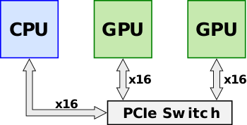
Announced in early 2014, NVLink was designed as an alternative solution to PCI Express with higher bandwidth and additional features (e.g., shared memory) specifically designed to be compatible with Nvidia's own GPU ISA for multi-GPU systems. Prior to the introduction of NVLink with Pascal (e.g., Kepler), multiple Nvidia's GPUs would sit on a shared PCIe bus. Although direct GPU-GPU transfers and accesses were already possible using Nvidia's Unified Virtual Addressing over the PCIe bus, as the size of data sets continued to grow, the bus became a growing system bottleneck. Throughput could further improve through the use of a PCIe switch.
NVLink is designed to replace the inter-GPU-GPU communication from going over the PCIe lanes. It's worth noting that NVLink was also designed for CPU-GPU communication with higher bandwidth than PCIe. Although it's unlikely that NVLink would be implemented on an x86 system by either AMD or Intel, IBM has collaborate with Nvidia to support NVLink on their POWER microprocessors. For support microprocessors, the NVLink can eliminate PCIe entirely for all links.
Links
A single NVLink is a bidirectional interface which comprises 8 differential pairs in each direction for a total of 32 wires. The pairs are DC coupled an use an 85Ω differential termination with an embedded clock. To ease routing, NVLink supports lane reversal and lane polarity, meaning the physical lane ordering and their polarity between the two devices may be reversed.
Packet
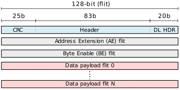
A single NVLink packet ranges from a one to eighteen flits. Each flit is 128-bit, allowing for the transfer of 256 bytes using a single header flit and 16 payload flits for a peak efficiency of 94.12% and 64 bytes using a single header flit and 4 data payload flits for an efficiency of 80% unidirectional. In bidirectional traffic, this is slightly reduced to 88.9% and 66.7% respectively.
A packet comprises of at least a header, and optionally, an address extension (AE) flit, a byte enable (BE) flit, and up to 16 data payload flits. A typical transaction has at least request and response with posted operations not necessitating a response.
Header flit
The header flit is 128-bit. It comprises a 25-bit CRC field (discussed below), 83-bit transaction field, and a 20-bit data link (DL) layer field. The transaction field includes the request type, address, flow control bits, and tag identifier. The data link field includes things such as the packet length, application number tag, and acknowledge identifier.
The address extension (AE) flit is reserved for fairly static bits and is usually transmitted only bits change.
Error Correction
Nvidia specifies the error rate at 1 in 1×10¹². Error detection is done through the 25-bit cyclic redundancy check header field. The receiver is responsible for keeping the data in a replay buffer. Transmitted packets are sequenced and a positive acknowledgment is sent back to the source upon a good CRC. A missing acknowledgment following a timeout will initiate a reply sequence, retransmitting all subsequent packets.
The CRC field consists of 25 bits, allowing up to 5 random bits in error for the largest packet or alternatively, for differential pair bursts it can support up to 25 sequential bit errors. CRC is actually calculated over the header and the previous payload, eliminating the need for a separate CRC field for the data payload. Note that since the header also incorporates the packet length, it is also gets included in the CRC check.
For example, consider a sequence of two data payload (32 bytes) flits and their accompanying header. The next packet will have the CRC done over the current header as well as the two data payload from the prior transaction. If this is the first transaction, the CRC assumes the prior transaction was a NULL transaction.
Data Rates
| NVLink 1.0 | NVLink 2.0 | |
|---|---|---|
| Signaling Rate | 20 GT/s | 25 GT/s |
| Lanes/Link | 8 | 8 |
| Rate/Link | 20 GB/s | 25 GB/s |
| BiDir BW/Link | 40 GB/s | 50 GB/s |
| Links/Chip | 4 (P100) | 6 (V100) |
| BiDir BW/Chip | 160 GB/s (P100) | 300 GB/s (V100) |
NVLink 1.0
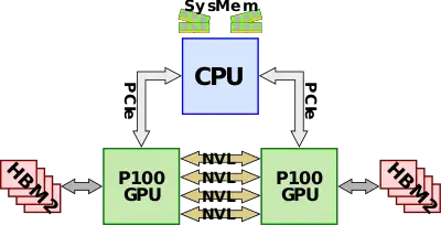
NVLink 1.0 was first introduced with the P100 GPGPU based on the Pascal microarchitecture. P100 comes with its own HBM memory in addition to being able to being able to access system memory from the CPU side. The P100 has four NVLinks, which supports up to 20 GB/s for a bidrectional bandwidth of 40 GB/s for a total aggregated bandwidth of 160 GB/s. In the most basic configuration, all four links are connected between the two GPUs for 160 GB/s GPU-GPU bandwidth in addition to the PCIe lanes connected to the CPU for accessing system DRAM.
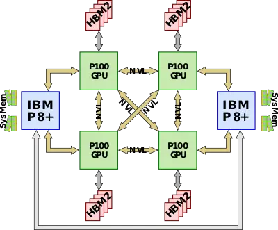
The first CPU to support NVLink natively was the IBM POWER8+ which allowed the NVLink interconnect to extend to the CPU, replacing the slower PCIe link. Since the P100 only has four NVLinks, a single link from each GPU can be used to link the CPU to the GPU. A typical full configuration node consists of four P100 GPUs and two Power CPUs. The four GPUs are fully connected to each other with the fourth link going to the CPU.
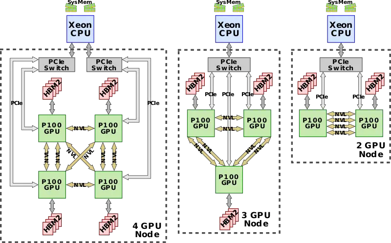
Since Intel-based CPUs do not support NVLinks (and are unlikely to ever support them), a couple of variations are possible from two to four P100 GPUs. In each configuration, the GPUs are all fully connected to each other with every two GPUs hooked up to a single PCIe switch which is directly connected to the CPU. Each link is 40 GB/s bidirectional regardless of the configuration and may be aggregated to provide higher bandwidth between any two GPUs the more links are used between them.
DGX-1 Configuration
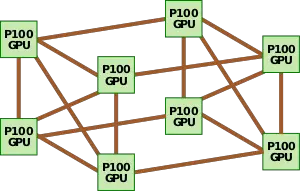
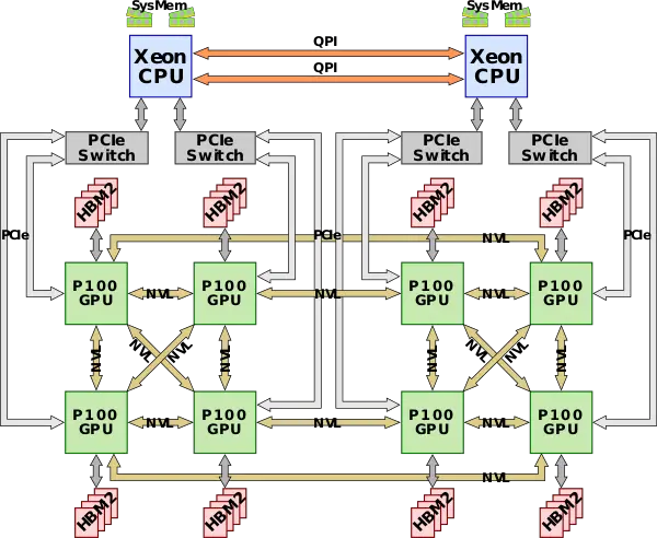
In 2017 Nvidia introduced the DGX-1 system which takes full advantage of NVLink. The DGX-1 consists of eight Tela P100 GPUs connected in a hybrid cube-mesh NVLink network topology along with dual-socket Xeon CPUs. The two Xeons communicate with each other over Intel's QPU while the GPUs communicate via the NVLink.
NVLink 2.0
NVLink 2.0 was first introduced with the V100 GPGPU based on the Volta microarchitecture along with IBM's POWER9. Nvidia added CPU mastering support, allowing both the GPU and CPU to access each others memory (i.e., direct load and stores) in a flat address space. The flat address space is supported through new address translation services. Additionally, there native support for atomic operations was added for both the CPU and GPU. With the addition of flat address space, NVLink now has cache coherence support, allowing the CPU to efficiently cache GPU memory, significantly improving latencies and thus performance. NVLink 2.0 has improved signaling rate to 25 Gbps per wire (25 GT/s) for 50 GB/s bidirectional bandwidth. The V100 also increased the number of NVLinks on-die to 6 for a total aggregated bandwidth of 300 GB/s. It's worth noting that additional power saving features were added such as deactivating lanes during idle.
NVLink 2.0 was introduced with the second-generation DGX-1, but the full topology change took place with the DGX-2. Nvidia also introduced the NVSwitch with the DGX-2 which is an 18 NVLink ports switch. The 2-billion transistor switch can route traffic from nine ports to any of the other nine ports. With 50 GB/s per port, the switch is capable of a total of 900 GB/s of bandwidth.
For the DGX-2, Nvidia uses six Template:nvlink to fully connect every one of the eight GPUs to all the other seven GPUs on the same baseboard.
References
- IEEE HotChips 29 (HC29), 2017
- IEEE HotChips 28 (HC28), 2016
