(→Core) |
(→FMA Unit) |
||
| Line 73: | Line 73: | ||
The FMA unit, called single-precision floating-point multiply-accumulators (FPMAC), is a nine-stage base-32 single-cycle accumulate algorithm using an intermediary carry-save with delayed addition. Three cycles are dedicated to the multiplier unit (S<sub>1</sub> - S<sub>3</sub> for four Wallace steps), a single cycle is for the sign inversion (S<sub>4</sub>) followed by a single cycle for the accumulation loop (S<sub>5</sub>). Finally, three stages are dedicated to the addition, normalization, and conversion back to base-2 steps (S<sub>6</sub>-S<sub>8</sub>). | The FMA unit, called single-precision floating-point multiply-accumulators (FPMAC), is a nine-stage base-32 single-cycle accumulate algorithm using an intermediary carry-save with delayed addition. Three cycles are dedicated to the multiplier unit (S<sub>1</sub> - S<sub>3</sub> for four Wallace steps), a single cycle is for the sign inversion (S<sub>4</sub>) followed by a single cycle for the accumulation loop (S<sub>5</sub>). Finally, three stages are dedicated to the addition, normalization, and conversion back to base-2 steps (S<sub>6</sub>-S<sub>8</sub>). | ||
| − | The unit takes in two {{arch|32}} [[IEEE-754]] [[single-precision]] operands | + | The unit takes in two {{arch|32}} [[IEEE-754]] [[single-precision]] operands and is designed to sustain a single FMA instruction every 250ps (4 GHz). The multiplier itself is a [[Wallace tree]] of 4-2 carry-save adders. In total, four Wallace tree stages are dedicated to the compression of partial product bits to a sum and carry and pair. Instead of the traditional carry propagate adder on the final stage, Intel retains the output in carry-save format and then converts the result to a base 32 at stage S<sub>3</sub> just before the accumulation. |
== Freya (SRAM) == | == Freya (SRAM) == | ||
Revision as of 12:21, 11 April 2018
| Edit Values | |
| Polaris µarch | |
| General Info | |
| Arch Type | CPU |
| Designer | Intel |
| Manufacturer | Intel |
| Introduction | February 2007 |
| Process | 65 nm |
| Core Configs | 80 |
| Pipeline | |
| Type | VLIW |
| Stages | 9 |
| Cache | |
| L1I Cache | 3 KiB/core |
| L1D Cache | 2 KiB/core |
| Succession | |
Polaris was a research microarchitecture designed by Intel Labs demonstarting the theoretical capabilities of a many-core chip performing 1 trillion floating point operations.
Contents
History
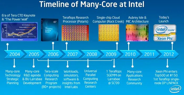
Intel originally announced and presented a Polaris wafer at the September 2006 Intel Developer Forum. Technical details were finally presented at IEEE ISSCC 2007. It was a concept project designed to demonstrate the potential of integrating many processing elements on a single silicon chip enabled by Moore's Law in order to achieve a high trillion floating point operations throughput. Polaris was Intel's first public chip as a direct consequence of their Tera-scale Computing Research Program and is the basis of Intel's later research projects which paved the way for Intel's Many Integrated Cores (MIC) architecture and the Xeon Phi many-core processor family.
Architecture
- ≥ 1 teraFLOPS (single-precision)
- ≥ 5 GHz clock
- 3D die stacking
- ≥ 1 TB/s bandwidth
- stacked SRAM
- 20 MiB, 256 KiB/core
- High efficiency
- Up to 27 GFLOPS/W with 310 GFLOPS
- network on a chip (NoC)
- mesh architecture
- 80 tiles
Block Diagram
Entire Chip
Individual Tile
System Overview
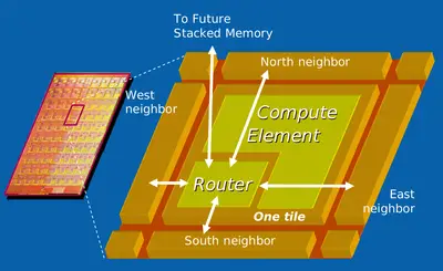
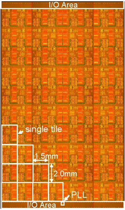
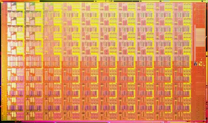
Polaris is a monolithic silicon consisting of 80 tiles arranged in a two-dimensional array of ten rows by eight columns. Each tile is effectively a core (Intel terms a processing engine (PE)) hooked to a router with mesochronous interfaces which is used to forward the packets between the tiles, allowing for clock-phase-insensitive tile-to-tile communication and synchronous operations within each tile. Tiles are linked to all four of their nearest neighbors as well as directly to the stacked SRAM memory.
Tile
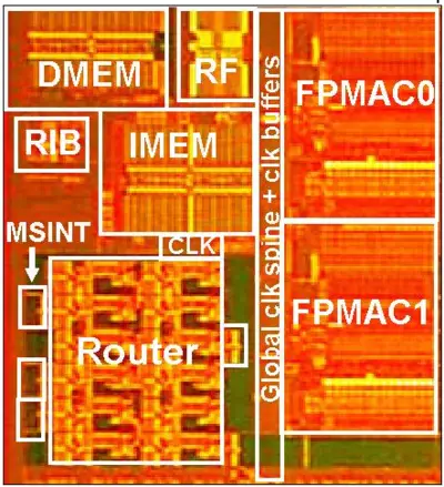
Each tile contains the core and the crossbar router.
Router
The underlying concept was to create a highly modular design which could scale from a low number of tiles to a large number of tiles without necessitating a large set of changes. Each tile is connected to a 5-port wormhole-switched router with mesochronous interfaces using two dead-lock free routing and a fully non-blocking crossbar switch with a total bandwidth of 80 GB/s at 4 GHz with a 1.25ns latency. Taking up a total area of just 0.34 mm², the router is connected to its four nearing neighbors - on the east, west, north, and south. The fifth port is designed to interface with the stacked SRAM which was located directly below the core itself. Links were designed with FIFO-based synchronization using a 4-deep circular FIFO which captures data using a delayed link strobe at the receiving end. Each lane has a 16 Flow control unIT (FLIT) queue, arbiter, and flow control logic. The router is implemented using a 5-stage pipeline with a two-stage round robin arbitration. On the first stage, an input port is bound to an output port in each lane and on the second stage, a spending FLIT is then selected from one of the two lanes. This means the same lanes are reused per-FLIT basis each time. The crossbar data bus is 36 bits wide and is double-pumped at the 4th pipe stage using a dual edge-trigged flip-flop, interleaving alternate data bits. This reduced the crossbar area by roughly 50%.
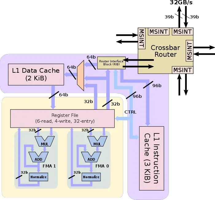
The entire on-chip network features a bisectional bandwidth of 256 GB/s. The router interface block (RIB) interfaces between the code and the router and performs the packet encapsulations. The architecture allows any core to send or receive instructions and data packets from and to any other core.
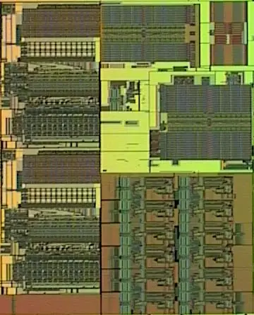
Core
The core, also called a processing engine (PE), executes 96-bit VLIWs encoding up to eight operations per cycle. The core contains two independent fused multiply-accumulates. Each FMA can sustain a multiply-add result (2 FLOPs) every cycle. Operating at 4 GHz, each core is capable of 16 GFLOPS, for a total chip peak performance of 1.28 TFLOPS.
There is a 3 KiB single-cycle instruction cache and a 2 KiB data cache. Each core has a single 32-entry register file with 10 ports (6 reads and 4 writes). A large number of ports allows for the simultaneous execution of a large set of operations such as scheduling to both FMAs, performing a load and store from the L1D$, program control, dynamic sleep instruction, and perform package sending/receiving from the network.
The two FMAs are implemented as fully-pipelined nine stages. This is implemented in nine stages using a single-cycle accumulate with base 32 and internal carry-save arithmetic and delay addition. To perform the single-cycle accumulate, the multiplier output carry-save format is kept and a Wallace tree of 4-2 carry-save adder accumulates the result in a temporary format. Intel claims this eliminated the need for a carry-propagate adder in the critical path. Additionally, since the accumulation is performed in base 32, the variable shifters were replaced by cheap constant shifters.
FMA Unit
The FMA unit, called single-precision floating-point multiply-accumulators (FPMAC), is a nine-stage base-32 single-cycle accumulate algorithm using an intermediary carry-save with delayed addition. Three cycles are dedicated to the multiplier unit (S1 - S3 for four Wallace steps), a single cycle is for the sign inversion (S4) followed by a single cycle for the accumulation loop (S5). Finally, three stages are dedicated to the addition, normalization, and conversion back to base-2 steps (S6-S8).
The unit takes in two 32-bit IEEE-754 single-precision operands and is designed to sustain a single FMA instruction every 250ps (4 GHz). The multiplier itself is a Wallace tree of 4-2 carry-save adders. In total, four Wallace tree stages are dedicated to the compression of partial product bits to a sum and carry and pair. Instead of the traditional carry propagate adder on the final stage, Intel retains the output in carry-save format and then converts the result to a base 32 at stage S3 just before the accumulation.
Freya (SRAM)
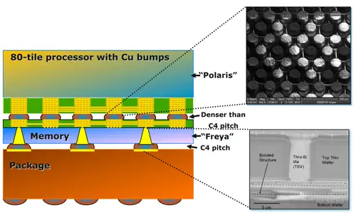
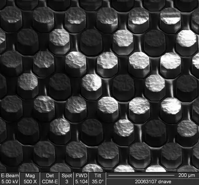
In order to provide a very high amount of bandwidth Intel had to move the memory very close to the CPU. Even placed next to the CPU die in the same package was not sufficient enough to provide the necessary bandwidth they were seeing. Stacked under the Polaris chip is a large SRAM (codename Freya) consisting of 256 KiB of memory per core for a total of 20 MiB. The connection between the dies uses a highly dense bumps. Intel reported the density to be roughly 4x that of the their 4C. It's worth noting that the reason the SRAM is placed under the CPU die is to allow proper heat dissipation for the CPU die through an active cooling solution on top.
The full chip uses 3,200 through-silicon vias. Using wafer-level stacking high-density interconnect could be realized, albeit at reduced flexibility and increased complexity. Overall a bandwidth of greater than 1 TB/s was demonstrated.
Clocking
The on-die PLL uses horizontal M8 and vertical M7 layers for clock distribution. Each layer consists of differential clocks for ow due-cycle variations along the worst-case clock route which is 26 mm. The differential clocks are converted to a single-ended clock at 50% due cycle using the opamp located at each of the tiles. At 4 GHz, 1.2 V supply is 2.2 W, helped by the simultaneous distribution of clock switching across the entire die.
Performance
Intel implemented key numerical algorithms from LAPACK on Polaris. Polaris, 110 °C, can achieve a maximum frequency of 3.125 GHz at 1 V for a peak performance of 1 teraFLOPS with a power consumption of 98 W. Alternatively, the chip can also do 4 GHz at 1.2 V for a performance of 1.28 TFLOPS and a power consumption of 181 W.
From a purely power-efficiency perspective, up to 27 GFLOPS/W can be achieved at 968.75 MHz at 0.6 V for a total performance of 310 GFLOPS. At that rating the chip power consumption is a mere 11 Watts.
| Power | Voltage | Frequency | Bisectional Bandwidth | Performance | Efficiency |
|---|---|---|---|---|---|
| 11 W | 0.6 V | 968.75 MHz | 496.64 Gb/s | 310 GFLOPS | 28.18 GFLOPS/W |
| 62 W | 0.95 V | 3.16 GHz | 1.62 Tb/s | 1.01 TFLOPS | 16.31 GFLOPS/W |
| 175 W | 1.2 V | 5.1 GHz | 2.61 Tb/s | 1.632 TFLOPS | 9.33 GFLOPS/W |
| 265 W | 1.35 V | 5.7 GHz | 2.92 Tb/s | 1,824 TFLOPS | 6.88 GFLOPS/W |
Die
Two different versions of the die were presented at a few different events. The exact difference is not known.
Variant 1
Chip
- Package LGA-1248
- 8,390 C4 solder bumps
- 14 layers organic substrate
- 343 signal pins
- 65 nm process
- 1 poly, 8 metal (Cu) layers
- 21.72 mm x 12.64 mm
- 274.54 mm² die size
- 100,000,000 transistors
- 96,000,000 tiles
- 1,200,000 transistors/tile
- 4,000,000 other
- 96,000,000 tiles
Tile
- 1.5 mm x 2.0 mm
- 3 mm² die size
Variant 2
Chip
- 65 nm process
- 1 poly, 8 metal (Cu) layers
- 22 mm x 13.75
- 302.5 mm² die size
Tile
Additional Shots
Additional die and wafer shots provided by Intel:
Documents
- Teraflops Research Chip
- Tera Tera Tera, 2006
- Polaris, MPSoC 2007
- Aim High, Intel Technical Update, Teratec ’07 Symposium, June 20, 2007
- Teraflops Research Chip Overview, Feb 2007
References
- Intel Developer Forum, September 2006
- IEEE ISSCC 2007
- IEEE Hot Chips 20 Symposium (HCS) 2008.
| codename | Polaris + |
| core count | 80 + |
| designer | Intel + |
| first launched | February 2007 + |
| full page name | intel/microarchitectures/polaris + |
| instance of | microarchitecture + |
| manufacturer | Intel + |
| microarchitecture type | CPU + |
| name | Polaris + |
| pipeline stages | 9 + |
| process | 65 nm (0.065 μm, 6.5e-5 mm) + |
