(stub page) |
|||
| Line 13: | Line 13: | ||
}} | }} | ||
'''Enhanced NetBurst''' (though no actual name was given by Intel) was a planned [[microarchitecture]] designed to succeed {{\\|NetBurst}}. On May 7 2004, Intel announced that they have cancelled the microarchitecture. | '''Enhanced NetBurst''' (though no actual name was given by Intel) was a planned [[microarchitecture]] designed to succeed {{\\|NetBurst}}. On May 7 2004, Intel announced that they have cancelled the microarchitecture. | ||
| + | |||
| + | == History == | ||
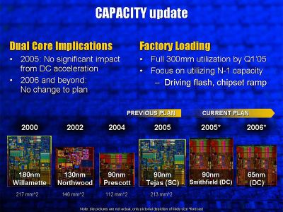
| + | [[File:tejas cancelled.jpg|right|400px]] | ||
| + | Slated to succeed {{\\|NetBurst}} in the second half of 2004, Intel first demonstrated this microarchitecture in early 2003 with samples expected to reach partners in the second half of the year. Although no actual name was given to the microarchitecture by Intel, at least not publicly, it was expected to feature a considerably longer pipeline over Netburst and thus feature incredibly high clock rates. At IDF in 2003 Intel suggested a clock rate in excess of 5 GHz on the [[90 nm process]] with around 8 to 9 GHz clock rate after a shrink to the [[65 nm process]]. | ||
| + | |||
| + | == Process Technology == | ||
| + | The Enhanced NetBurst microarchitecture was planned to be manufactured initially on a [[90 nm process]] with faster models after a [[process shrink]] to a [[65 nm process]]. | ||
== Codenames == | == Codenames == | ||
| Line 22: | Line 29: | ||
| {{intel|Jayhawk |l=core}} || Server microprocessors | | {{intel|Jayhawk |l=core}} || Server microprocessors | ||
|} | |} | ||
| + | |||
| + | == Architecture == | ||
| + | This microarchitecture was designed to deliver considerably higher clock speed by elongating the NetBurst's pipeline. | ||
| + | === Key changes from {{\\|NetBurst}} === | ||
| + | * Very long pipeline | ||
| + | ** 40-50+ stages | ||
| + | * Higher clock speeds | ||
| + | ** 5 GHz+ on a [[90 nm process]] | ||
| + | ** 8-9 GHz+ on a [[65 nm process]] | ||
| + | * New Instructions | ||
| + | ** Tejas New Instructions (TNI) (later renamed to {{x86|SSSE3}}) | ||
Revision as of 20:37, 12 August 2017
| Edit Values | |
| Enhanced NetBurst µarch | |
| General Info | |
| Arch Type | CPU |
| Designer | Intel |
| Manufacturer | Intel |
| Process | 90 nm, 65 nm |
| Succession | |
Enhanced NetBurst (though no actual name was given by Intel) was a planned microarchitecture designed to succeed NetBurst. On May 7 2004, Intel announced that they have cancelled the microarchitecture.
History
Slated to succeed NetBurst in the second half of 2004, Intel first demonstrated this microarchitecture in early 2003 with samples expected to reach partners in the second half of the year. Although no actual name was given to the microarchitecture by Intel, at least not publicly, it was expected to feature a considerably longer pipeline over Netburst and thus feature incredibly high clock rates. At IDF in 2003 Intel suggested a clock rate in excess of 5 GHz on the 90 nm process with around 8 to 9 GHz clock rate after a shrink to the 65 nm process.
Process Technology
The Enhanced NetBurst microarchitecture was planned to be manufactured initially on a 90 nm process with faster models after a process shrink to a 65 nm process.
Codenames
| Codename | Target |
|---|---|
| Tejas | Desktop microprocessors |
| Jayhawk | Server microprocessors |
Architecture
This microarchitecture was designed to deliver considerably higher clock speed by elongating the NetBurst's pipeline.
Key changes from NetBurst
- Very long pipeline
- 40-50+ stages
- Higher clock speeds
- 5 GHz+ on a 90 nm process
- 8-9 GHz+ on a 65 nm process
- New Instructions
- Tejas New Instructions (TNI) (later renamed to SSSE3)
| codename | Enhanced NetBurst + |
| designer | Intel + |
| full page name | intel/microarchitectures/enhanced netburst + |
| instance of | microarchitecture + |
| manufacturer | Intel + |
| microarchitecture type | CPU + |
| name | Enhanced NetBurst + |
| process | 90 nm (0.09 μm, 9.0e-5 mm) + and 65 nm (0.065 μm, 6.5e-5 mm) + |
