From WikiChip
Difference between revisions of "ibm/microarchitectures/z14"
| Line 19: | Line 19: | ||
|l1i=128 KiB | |l1i=128 KiB | ||
|l1d=128 KiB | |l1d=128 KiB | ||
| − | |predecessor= | + | |predecessor=z13 |
|predecessor link=ibm/microarchitectures/z13 | |predecessor link=ibm/microarchitectures/z13 | ||
}} | }} | ||
Revision as of 18:18, 20 July 2017
| Edit Values | |
| z14 µarch | |
| General Info | |
| Arch Type | CPU |
| Designer | IBM |
| Manufacturer | GlobalFoundries |
| Introduction | July 17, 2017 |
| Process | 14 nm |
| Core Configs | 7, 8, 9, 10 |
| Pipeline | |
| Type | Superscalar, Pipelined |
| OoOE | Yes |
| Speculative | Yes |
| Reg Renaming | Yes |
| Instructions | |
| ISA | z/Architecture |
| Cache | |
| L1I Cache | 128 KiB |
| L1D Cache | 128 KiB |
| Succession | |
z14 was a z/Architecture-based microarchitecture designed by IBM and introduced in 2017 for their z14 processors and mainframes. The z14 microarchitecture replaced the z13.
Contents
Process Technology
z14-based microprocessors are manufactured on GlobalFoundries's 14 nm (14HP) FinFET Silicon-On-Insulator (SOI) process. The process was designed by IBM at what used to be their East Fishkill, New York fab which has since been sold to GlobalFoundries.
Architecture
Key changes from z13
- 14 nm process (from 22 nm)
- Higher clock frequency (5.2 GHz from 5 GHz)
- Higher scalability
- Up to 170-way multiprocessing (from 141-way)
- Core
- Improved Operand Store Compare (OSC) prediction
- Faster branch wakeup
- Improved instruction delivery
- Cache
- New directory design
- Power efficient
- L1I$ increased to 128 KiB/core (from 96 KiB/core; 33% increase)
- L2D$ increased to 4 MiB/core (from 2 MiB/core; 100% increase)
- L3$ increased to 128 MiB/CP (from 64 MiB/CP; 100% increase)
- New 672 MiB/drawer of shared L4
- New directory design
- Central Processor Assist for Cryptographic Function (CPACF)
- Dedicated co-processor for each core
- Claims 6x faster encryption functions (vs. z13)
- 4x Advanced Encryption Standard (AES) speedup
- Support for True Random Number Generator
- New support for SHA-3 standard
| This section requires expansion; you can help adding the missing info. |
Overview
| This section is empty; you can help add the missing info by editing this page. |
Die
Core
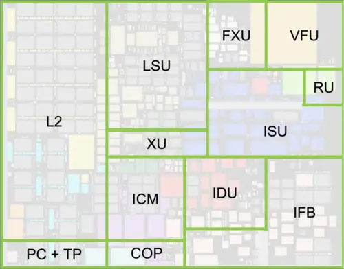
Below is a layout of a single physical core:
- L2 - L2I$ + L2D$
- PC + TP - Core pervasive unit (instrumentation/error collection) + Trap
- LSU - Load-store unit (+ L1D$)
- XU - Translation unit (TLB + DAT)
- ICM - Instruction cache & merge
- COP - Dedicated Co-Processor
- FXU - Fixed-point unit
- VFU - Vector and Floating point Unit
- ISU - Instruction sequence unit
- RU - Recovery unit
- IDU - Instruction decode unit
- IFB - Instruction fetch and branch prediction
Single-chip module (SCM)
IBM's z14 Single-Chip Module (SCM) consists of a multi-layer metal substrate module that includes either:
- 1x Processor Unit (PU)
- 1x System Controller (SC)
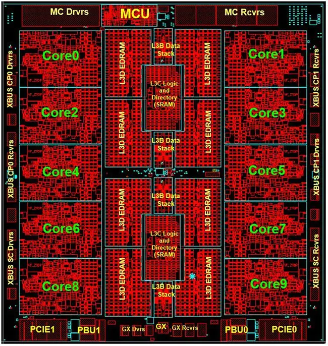
Processor Unit (PU) Chip
- IBM's developed (now GlobalFoundries) 14HP Process
- CMOS FinFET SOI
- 17 Metal Layers
- 25.3 x 27.5 mm die
- 695.75 mm² die size
- deca-core
- 5.2 GHz (192 ps cycle time)
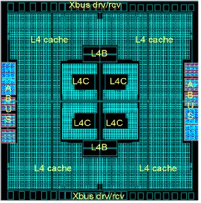
System Controller (SC) Chip
- IBM's developed (now GlobalFoundries) 14HP Process
- CMOS FinFET SOI
- 17 Metal Layers
- 25.3 x 27.5 mm die
- 695.75 mm² die size
- 7,100,000,000 transistors
- + 2,100,000,000 cells of eDRAM (~2.1B xTors + 2.1B capacitors)
- 672 MiB shared eDRAM L4 Cache
Facts about "z14 - Microarchitectures - IBM"
| codename | z14 + |
| core count | 7 +, 8 +, 9 + and 10 + |
| designer | IBM + |
| first launched | July 17, 2017 + |
| full page name | ibm/microarchitectures/z14 + |
| instance of | microarchitecture + |
| instruction set architecture | z/Architecture + |
| manufacturer | GlobalFoundries + |
| microarchitecture type | CPU + |
| name | z14 + |
| process | 14 nm (0.014 μm, 1.4e-5 mm) + |


