(→Architecture) |
(→Core) |
||
| Line 75: | Line 75: | ||
In conjunction with the address register is a dedicated incrementer which calculates the next address. The actual address for the next instruction will usually come from that incrementer. However, occasionally, the next instruction may also come from the [[ALU]] instead. On very rare occasions, the next instruction value can be forced to an exception. When the instruction is coming from the incrementer, the ARM1 will also assert this on the <code>SEQ</code> pin, allowing the external memory controller to know that the next instruction will in fact be +4 the current instruction, allowing it to determine if an address translation is necessary and prepare ahead. This is done to improve performance because it can make use of [[Page-Mode DRAM]], allowing for more efficient consecutive memory reads. | In conjunction with the address register is a dedicated incrementer which calculates the next address. The actual address for the next instruction will usually come from that incrementer. However, occasionally, the next instruction may also come from the [[ALU]] instead. On very rare occasions, the next instruction value can be forced to an exception. When the instruction is coming from the incrementer, the ARM1 will also assert this on the <code>SEQ</code> pin, allowing the external memory controller to know that the next instruction will in fact be +4 the current instruction, allowing it to determine if an address translation is necessary and prepare ahead. This is done to improve performance because it can make use of [[Page-Mode DRAM]], allowing for more efficient consecutive memory reads. | ||
| + | |||
| + | ==== Decode ==== | ||
| + | {{empty section}} | ||
| + | |||
| + | ==== Execute ==== | ||
| + | {{empty section}} | ||
== Die Shot == | == Die Shot == | ||
Revision as of 18:57, 24 June 2017
| Edit Values | |
| ARM1 µarch | |
| General Info | |
| Arch Type | CPU |
| Designer | ARM Holdings |
| Manufacturer | VLSI Technology |
| Introduction | 1985 |
| Process | 3 µm |
| Core Configs | 1 |
| Pipeline | |
| Type | Scalar, Pipelined |
| Stages | 3 |
| Decode | 1-way |
| Instructions | |
| ISA | ARMv1 |
| Cache | |
| L1I Cache | 0 KiB/Core |
| L1D Cache | 0 KiB/Core |
| Succession | |
ARM1 was the first ARM microarchitecture implemented by ARM Holdings (then Acorn Computers) as a research and development project for the BBC Computer Literacy Project. ARM1 was introduced in 1985 and was extended to be used as a coprocessor in the Acorn's BBC Micro microcomputers. ARM1 was distributed as an evaluation system and was never commercialized.
Contents
History
- Main article: ARM's History
The ARM1 (Acorn RISC Machine 1) is Acorn Computers' first microprocessor design. The ARM1 was the initial result of the Advanced Research and Development division Acorn Computers formed in order to advance the development of their own RISC processor. The ARM instruction set design started in 1983. A reference model was written in BBC BASIC by Sophie Wilson and Steve Furber in just 808 lines of code. On April 26 1985, after 6 man-years of design effort, the first ARM processor prototype was delivered. The first batch of prototypes were functional and were shipped to customers in the form of evaluation systems. At that time the ARM1 was the simplest RISC processor produced.
The first prototype tested worked on the first try, this was despite the ammeter reading no power. The prototype test board designed was faulty with a short. The chip was entirely running off the leakage from the I/Os. Designed to run at 1 W, the chip averaged under 100 mW typical power.
Process Technology
- See also: 3 µm process
ARM1 chips were manufactured by VLSI Technology on a 3 µm double-level metal CMOS process.
Architecture
The ARM1 is based on the ARMv1 ISA which is an entirely clean-sheet 32-bit RISC design.
Overview
- 3 µm process
- Implements ARMv1
- Goal 1.5x performance of the VAX 11/780
- 26-bit address space
- Pipeline
- Very simple
- 3-stage
- No hardware multiplication
- 25 32-bit registers
- 16 For user
- 9 For supervisor
- 4 Modes
- User, Supervisor, IRQ, FIQ
Block Diagram
| This section is empty; you can help add the missing info by editing this page. |
Core
The ARM1 is an extremely simple 32-bit single-chip RISC microprocessor implementation.
Pipeline
The ARM1 utilizes a pipelining technique in order to improve performance and efficiency. The ARM1's pipeline consists of 3 states:
The ARM1 operates on a guaranteed non-overlapping two-phase clock which allowed for level-triggered transfer instead of edge-triggering. The two clock phases are not generated on-die but come from an external oscillator. A complete cycle on the ARM1 is therefore Φ1 + Φ2.
Fetch
The Instruction Pipe is a functional block that holds awaiting instructions until execution, it therefore holds a number of instruction sufficient to ensure instructions are always executing at all cycles on all stages.
The program counter on the ARM1 always points to the instruction being fetched. That is, with every instruction being exactly 4 bytes, the currently executing instruction is always PC - 8. During the fetch stage, the address specified by the address register gets sent through the address pins and is fetched from memory.
In conjunction with the address register is a dedicated incrementer which calculates the next address. The actual address for the next instruction will usually come from that incrementer. However, occasionally, the next instruction may also come from the ALU instead. On very rare occasions, the next instruction value can be forced to an exception. When the instruction is coming from the incrementer, the ARM1 will also assert this on the SEQ pin, allowing the external memory controller to know that the next instruction will in fact be +4 the current instruction, allowing it to determine if an address translation is necessary and prepare ahead. This is done to improve performance because it can make use of Page-Mode DRAM, allowing for more efficient consecutive memory reads.
Decode
| This section is empty; you can help add the missing info by editing this page. |
Execute
| This section is empty; you can help add the missing info by editing this page. |
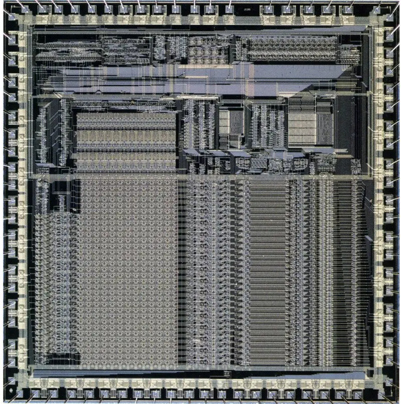
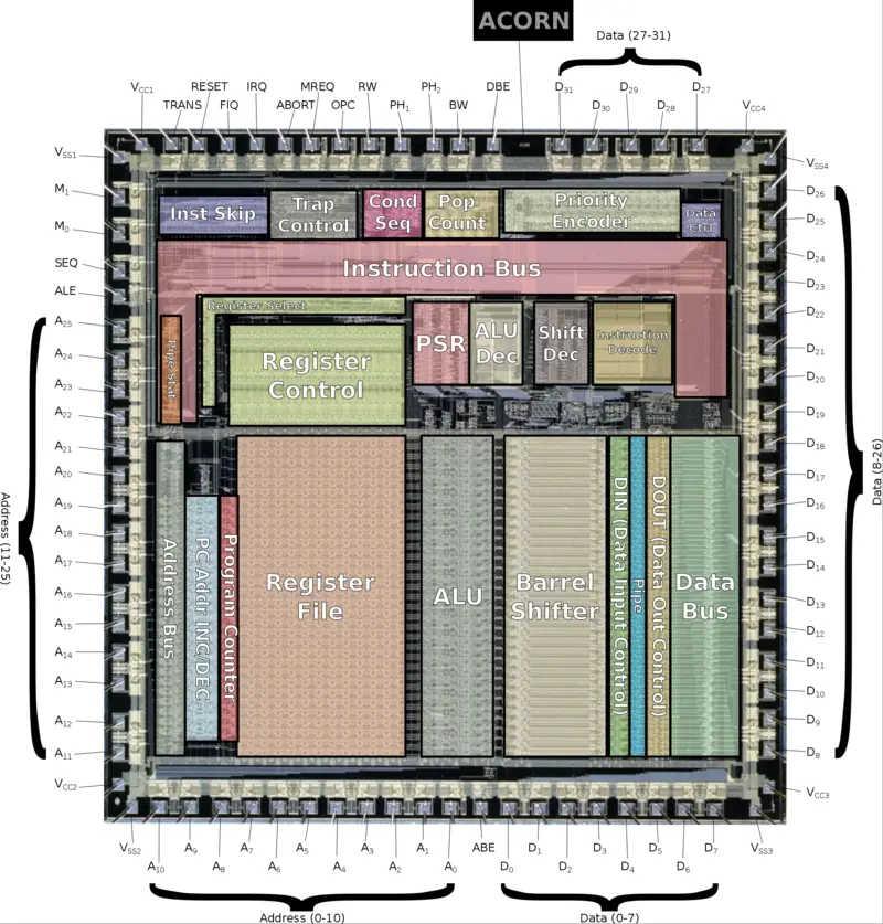
Die Shot
- 3 µm process
- 24,800 transistors
- ~6,000 gates
- ~7 mm x 7mm
- 50 mm² die size
- PLCC-82 (Plastic leaded chip carrier)
- 74 signal pins
- 8 power/ground pins
All ARM1 Chips
| This section is empty; you can help add the missing info by editing this page. |
References
- ARM hardware reference manual, ARM Evaluation System, Acorn OEM Products, August 1986
Documents
| This section is empty; you can help add the missing info by editing this page. |
| codename | ARM1 + |
| core count | 1 + |
| designer | ARM Holdings + |
| first launched | 1985 + |
| full page name | acorn/microarchitectures/arm1 + |
| instance of | microarchitecture + |
| instruction set architecture | ARMv1 + |
| manufacturer | VLSI Technology + |
| microarchitecture type | CPU + |
| name | ARM1 + |
| pipeline stages | 3 + |
| process | 3,000 nm (3 μm, 0.003 mm) + |


