(→Process Technology) |
(→Process Technology) |
||
| Line 28: | Line 28: | ||
== Process Technology == | == Process Technology == | ||
| − | Cannonlake is manufactured on Intel's [[10 nm process]] (P1274) | + | Cannonlake is manufactured on Intel's [[10 nm process]] (P1274). Intel's 10 nm process is the high-volume manufacturing process to employ [[Self-Aligned Quad Patterning]] (SAQP). Intel's 10nm features a 0.0367 µm² [[SRAM]] bit cell. |
| − | Scaling: | + | [[Scaling]]: |
{| class="wikitable" | {| class="wikitable" | ||
|- | |- | ||
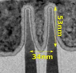
| − | ! !! Broadwell !! Cannonlake !! Δ | + | ! !! Broadwell !! Cannonlake !! Δ !! rowspan="8" | [[File:intel 10nm fin.png|250px]] |
|- | |- | ||
| || [[14 nm]] || [[10 nm]] || | | || [[14 nm]] || [[10 nm]] || | ||
|- | |- | ||
| − | | Fin Pitch || 42 nm || 34 | + | | Fin Pitch || 42 nm || 34 || 0.81x |
| + | |- | ||
| + | | Fin Width || 8 nm || ? nm || ?x | ||
| + | |- | ||
| + | | Fin Height || 42 nm || 53 nm || 1.24x | ||
|- | |- | ||
| Gate Pitch || 70 nm || 54 nm || 0.77x | | Gate Pitch || 70 nm || 54 nm || 0.77x | ||
| Line 46: | Line 50: | ||
| Cell Height || 399 nm || 272 nm || 0.68x | | Cell Height || 399 nm || 272 nm || 0.68x | ||
|} | |} | ||
| − | |||
== Codenames == | == Codenames == | ||
Revision as of 18:34, 29 March 2017
| Edit Values | |
| Cannonlake µarch | |
| General Info | |
| Arch Type | CPU |
| Designer | Intel |
| Manufacturer | Intel |
| Introduction | 2017 |
| Process | 10 nm |
| Cores | |
| Core Names | Cannonlake Y, Cannonlake U |
| Succession | |
Cannonlake (CNL) (formerly Skymont) is a planned microarchitecture by Intel as a successor to Kaby Lake. Cannonlake is expected to be fabricated using a 10 nm process and is set to be introduced in the fourth quarter of 2017. Cannonlake is the "Process" microarchitecture as part of Intel's PAO model.
For desktop and mobile, Cannonlake is expected to be branded as 8th Generation Intel Core i3, Core i5. and Core i7 processors. For server class processors, Intel is expected to brand it as Xeon E3 v7, Xeon E5 v7, and Xeon E7 v7.
Contents
Process Technology
Cannonlake is manufactured on Intel's 10 nm process (P1274). Intel's 10 nm process is the high-volume manufacturing process to employ Self-Aligned Quad Patterning (SAQP). Intel's 10nm features a 0.0367 µm² SRAM bit cell.
| Broadwell | Cannonlake | Δ | 
| |
|---|---|---|---|---|
| 14 nm | 10 nm | |||
| Fin Pitch | 42 nm | 34 | 0.81x | |
| Fin Width | 8 nm | ? nm | ?x | |
| Fin Height | 42 nm | 53 nm | 1.24x | |
| Gate Pitch | 70 nm | 54 nm | 0.77x | |
| Interconnect Pitch | 52 nm | 36 nm | 0.69x | |
| Cell Height | 399 nm | 272 nm | 0.68x |
Codenames
| Core | Abbrev | Description | Graphics | Target |
|---|---|---|---|---|
| Cannonlake Y | CNL-Y | Extremely low power | GT2 | 2-in-1s detachable, tablets, and computer sticks |
| Cannonlake U | CNL-U | Ultra-low Power | GT2 | Light notebooks, portable All-in-Ones (AiOs), Minis, and conference room |
Architecture
| This section is empty; you can help add the missing info by editing this page. |
Key changes from Kaby Lake
- 10 nm process (from 14 nm)
- 300 Series chipset
All Cannonlake Chips
| Cannonlake Chips | |||||||||||||||||||||||
|---|---|---|---|---|---|---|---|---|---|---|---|---|---|---|---|---|---|---|---|---|---|---|---|
| Main processor | IGP | Major Feature Diff | |||||||||||||||||||||
| Model | Launched | Price | Family | Platform | Core | C | T | L3$ | L4$ | TDP | Freq | Turbo | Max Mem | Name | Freq | Turbo | TBT | HT | AVX2 | TXT | TSX | vPro | VT-d |
| Uniprocessors | |||||||||||||||||||||||
| No Cannonlake Chips have been released yet. | |||||||||||||||||||||||
| Count: 0 | |||||||||||||||||||||||
See also
- AMD's Zen
| codename | Cannonlake + |
| designer | Intel + |
| first launched | 2017 + |
| full page name | intel/microarchitectures/cannon lake + |
| instance of | microarchitecture + |
| manufacturer | Intel + |
| microarchitecture type | CPU + |
| name | Cannonlake + |
| process | 10 nm (0.01 μm, 1.0e-5 mm) + |