m (→Discrete Chips) |
m (→Design) |
||
| Line 27: | Line 27: | ||
For 2, 4, and 8-input multiplexers the equations are thus: | For 2, 4, and 8-input multiplexers the equations are thus: | ||
| − | :<math>\text{MUX21}(a, b) = (A\overline{S_0})+(BS_0) | + | :<math> |
| − | + | \begin{align} | |
| − | + | \text{MUX21}(a, b) &= (A\overline{S_0})+(BS_0) \\ | |
| + | \text{MUX41}(a, b, c, d) &= (A\overline{S_0 S_1})+(B\overline{S_0}S_1)+(C S_0\overline{S_1})+(D S_0 S_1) \\ | ||
| + | \text{MUX81}(a, b, c, d, e, f, g) &= (A\overline{S_0 S_1 S_2})+(B\overline{S_0 S_1}S_2)+(C \overline{S_0} S_1 \overline{S_2})+(D \overline{S_0} S_1 S_2)+(E S_0 \overline{S_1 S_2})+(F S_0 S_1 \overline{S_2})+(G S_0 S_1 S_2) | ||
| + | \end{align} | ||
| + | </math> | ||
{{clear}} | {{clear}} | ||
| + | |||
== Implementations == | == Implementations == | ||
Many different variations of multiplexers exist. Typically larger multiplxers (over 8 or 16 inputs) are built using smaller multiplxers using a [[/tree|multiplexer tree]]. | Many different variations of multiplexers exist. Typically larger multiplxers (over 8 or 16 inputs) are built using smaller multiplxers using a [[/tree|multiplexer tree]]. | ||
Revision as of 03:39, 24 December 2015
| Multiplexer | ||||||||||||||||||||||||||||
| Typical Symbol (2:1 MUX) | ||||||||||||||||||||||||||||
| Functional | ||||||||||||||||||||||||||||
| Truth Table | ||||||||||||||||||||||||||||
| ||||||||||||||||||||||||||||
| ||||||||||||||||||||||||||||
| ||||||||||||||||||||||||||||
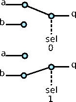
A multiplexer (mux) or a data selector or input selector is a combinational circuit device that selects one of N inputs and provides it on its output. A set of inputs called select lines determine which input should be passed to the output. For a 2:1 (two-to-one) MUX, when sel is 0, q = a and when sel is 1, q = b. A multiplexer with 2N input lines requires N select lines.
Multiplexers are useful in any application in which data must be chosen from multiple sources to a single destination. Multiplexers are also heavily used in I/O operations, data buses, and register files. Additionally multiplexers have also found their way to various other circuits such as adders.
Contents
Description
 A multiplxer is a device that receives multiple inputs from usually different sources. A set of select lines are then used to choose which of those inputs gets produced as output. Signals to the select lines usually come from a control unit that determins which, if any, of the signals should be routed to some destination. MUXes are core components in most digital systems as they can be used to pass the correct signal based on some conditional logic. For example, consider a data bus that is connected to multiple memory storage units. One can use a multiplexer to select which of those lines should be going to the shared data bus.
Enable/Tri-State
It's often desirable to add an enable (or strobe) input EN to a multiplexer. An enable input makes the multiplexer operate. When EN = 0, the output is High-Z or less commonly LOW (depending on the specific device). When EN = 1, the multiplexer performs its operation depending on the selection line.
Tri-state multiplexers are MUXes that do not force a LOW when enable is 0 but instead go into a High-Z state. Those types of multiplexers can be hooked up directly to a shared bus ensuring that only one signal is being generated on the bus at any given time.
Design
For a multiplexer with inputs, you also need selection lines. It does mean that for multiplexers with odd number of inputs, some selection line combinations are not allowed (e.g. in a 3:1 MUX, the SEL=11 combination is not allowed). MUXes in the form :1 can be expressed by
Where is the kth minterm of the variable.
For 2, 4, and 8-input multiplexers the equations are thus:
Implementations
Many different variations of multiplexers exist. Typically larger multiplxers (over 8 or 16 inputs) are built using smaller multiplxers using a multiplexer tree.
2:1 MUX (MUX21)
| 2:1 Mux | |||
|---|---|---|---|
| Sel | A | B | Q |
| 0 | 0 | X | 0 |
| 0 | 1 | X | 1 |
| 1 | X | 0 | 0 |
| 1 | X | 1 | 1 |

The simplest multiplexer is the 2:1 MUX (or MUX21) which simply selects its output from just two possible inputs. Its selection lines is therefore made of a single bit. A truth table is provided on the right.
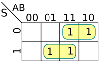
The K-Map for that truth table is provided on the left. From there the sum of minterms and the logic function for a 2:1 MUX can be derived.
CMOS
A very fast and compact, CMOS-based PTL logic, 2:1 MUX device can be built using two transmission gates as shown below. The top transmission gate controls if the input from A should pass to the output while the bottom transmission gate does the same for the B input. A single inverter is used to invert the selection line value to one of the gates so that only one of them (e.i. input A or input B) is allowed to pass. While smaller overall, this multiplexer is also nonrestoring.
 |

|
| This section requires expansion; you can help adding the missing info. |
A 2:1 MUX can also be built using an AOI222 gate.
3:1 MUX
| This section is empty; you can help add the missing info by editing this page. |
4:1 Mux
| Sel<0> | Sel<1> | I<0> | I<1> | I<2> | I<3> | Q |
|---|---|---|---|---|---|---|
| 0 | 0 | 0 | X | X | X | 0 |
| 0 | 0 | 1 | X | X | X | 1 |
| 0 | 1 | X | 0 | X | X | 0 |
| 0 | 1 | X | 1 | X | X | 1 |
| 1 | 0 | X | X | 0 | X | 0 |
| 1 | 0 | X | X | 1 | X | 1 |
| 1 | 1 | X | X | X | 1 | 1 |
| 1 | 1 | X | X | X | 0 | 0 |
A 4:1 Multiplexer is a common multiplexer that takes selects one input among 4 and connects it to its output based on a 2-bit select line. There are many way to construct a 4:1 Mux, one possibility is using 2:1 Mux as shown below:
Alternatively, a 4:1 Mux can be built out of basic gates. Its function is shown below:
Q =
Where A, B, C, and D are the four inputs. Q is the output.
CMOS
| This section is empty; you can help add the missing info by editing this page. |
8:1 MUX
| This section is empty; you can help add the missing info by editing this page. |
Large Multiplexers
- Main article: Multiplexer Tree
Multiplexers generally only come in a few common sizes. Even in ASIC design, arbitrary sized multiplexers are not always offered. Large multiplexers can always be built from a collection of smaller ones. Consider a register file with 32 registers where we only want to select a single register at any given time. Such multiplexer can be design from four 8:1 Mux.
Discrete Chips
Various multiplexers are available in discrete chips as well for both 7400 series and 4000 series.
7400 series chips
| Device Number | Name | Description |
|---|---|---|
| 74150 | 16:1 MUX | Output is inverted input |
| 74151 | 8:1 MUX | Output is inverted input |
| 74151A | 8:1 MUX | Output is inverted input |
| 74152 | 8:1 MUX | Complementary outputs |
| 74153 | Dual 4:1 MUX | Output same as input |
| 74157 | Quad 2:1 MUX | Output same as input |
| 74158 | Quad 2:1 MUX | Output is inverted input |
| 74298 | Quad 2:1 MUX with Register | MUX with an SR latch |
| 74399 | Quad 2:1 MUX with Register | MUX with an SR latch |
| 74398 | Quad 2:1 MUX with Register | MUX with an SR latch / Complementary outputs |
4000 series chips
| Device Number | Name | Description |
|---|---|---|
| 4512 | 8:1 MUX with EN | Output same as input, High-Z Enable |
| 4514 | 16:1 MUX with EN/Register | Output same as input |
| 4515 | 16:1 MUX with EN/Register | Output is inverted input |
| 4539 | Dual 4:1 MUX | Output same as input |
| 40257 | Quad 2:1 MUX with EN | Complementary outputs, High-Z Enable |
74151 - 8:1 Mux
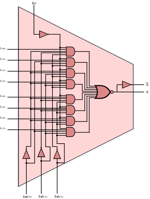
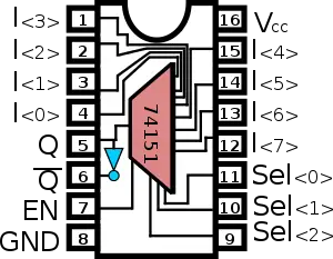
A common multiplexer is the 8:1 Mux which selects one of 8 bits of input. The 74151 is a popular 16-pin DIP IC that implements an 8:1 mux. Note that the implementation below is an active-low.
To the right is the typical schematic of the 74151, 16-pin DIP IC. Vcc is on pin 16 and GND is on pin 8. Pins 5 and 6 are the outputs, the output on pin 6 is the inverted version of the output on pin 5. The enable is on pin 7.
| 8:1 Mux | |||||
|---|---|---|---|---|---|
| Inputs | Output | ||||
| Select | Enable | ||||
| Sel<0> | Sel<1> | Sel<2> | EN | Q | Q |
| X | X | X | 1 | 1 | 0 |
| 0 | 0 | 0 | 0 | I<0> | I<0> |
| 0 | 0 | 1 | 0 | I<1> | I<1> |
| 0 | 1 | 0 | 0 | I<2> | I<2> |
| 0 | 1 | 1 | 0 | I<3> | I<3> |
| 1 | 0 | 0 | 0 | I<4> | I<4> |
| 1 | 0 | 1 | 0 | I<5> | I<5> |
| 1 | 1 | 0 | 0 | I<6> | I<6> |
| 1 | 1 | 1 | 0 | I<7> | I<7> |


