An Inverter or a NOT gate, is a logic gate which implements logical negation. When the input is LOW, the output is HIGH and when the input is HIGH, the output is LOW. Inverters are the nucleus of all digital systems. Understanding its operation, behavior, and properties for a specific process makes it possible to expand its design onto more complex structures such as NOR and NAND gates. The electrical behavior of much bigger and complex circuitry can be derived by extrapolating the behavior observed from simple inverters.
Contents
Functionality[edit]
An inverter generates a signal that is logically opposite to its input. When the input is sufficiently LOW, the output generate is HIGH. Likewise, when the input is sufficiently HIGH, the output generate becomes LOW.
Expression:
Q = A = ¬A
| NOT Gate | |
|---|---|
| A | Q |
| 0 | 1 |
| 1 | 0 |
Standard symbols[edit]
Below are the three standard symbols that represent the NOT gate:
| Standard Symbols | ||
|---|---|---|
| ANSI | IEC | DIN |
 |
 |

|
Implementation[edit]
An inverter can be implemented using various transistor technologies.
CMOS Inverter[edit]
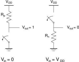
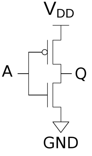
A static CMOS inverter can be constructed from a single nMOS transistor and a single pMOS transistor. As usual, the pMOS is connected to VDD and nMOS is connected to ground. When the input is LOW, the nMOS transistor is off and the pMOS transistor is on. The output is pulled up to HIGH as it's connected to VDD but not GND. When the input is HIGH, the nMOS transistor is on and the pMOS transistor is off yielding an output that is connected to GND. CMOS inverters are typically used to drive other MOS devices by connecting a capacitor on the output end; the capacitor is charged and discharged during each switch.
| Steady State Response | G = 0 | G = 1 | |
|---|---|---|---|
 |
VOL = 0 VOH = VDD VM = f(Rn, Rp) |

|

|
The Vth point of a CMOS inverter can be approximated using the expression \( V_{th} = \frac{V_{DD}-|V_{tp}|+V_{th}\sqrt{\frac{K_n}{K_p}}}{1+\sqrt{\frac{K_n}{K_p}}} \) where \( V_{tn} \) and \( V_{tp} \) are the threshold voltages for nMOS and pMOS devices. \( K_n = (\frac{W}{L})_n \centerdot µ\text{N Cox} \) and \( K_p = (\frac{W}{L})_p \centerdot µ\text{P Cox} \). This equation, however, requires caution as it's not practical for the design process due to non-ideal effects (eg. short-channel effects). The static power dissipation during logic 0 and logic 1 are almost zero because \( i_{DP} = i_{DN} = 0 \). When the input is LOW, pMOS is conducting and nMOS is off; the load capacitor is charged via the pMOS device.The power dissipated in the pMOS transistor is \( P_p = i_LV_{P} = i_L(V_{DD}-V_O) \). Likewise, the current can be related by \( i_L = \frac{C_Ldv_O}{dt} \). The energy dissipation in the pMOS device can be expressed as the output switches from LOW to HIGH,
, where \( E_p \) is the energy stored in capacitor \( C_L \) during HIGH output.
When the inverter's input is HIGH and the output is LOW, all the energy stored in the load capacitor is dissipated in the nMOS device because during that time the pMOS is cut off and the nMOS device is conducting. Therefore the energy dissipated in the nMOS device can be expressed as \( E_n = \frac{1}{2}C_LV_{DD}^2 \). During one complete switch cycle the total energy is the sum of both transistors: \( E_T = E_p + E_n = \frac{1}{2}C_LV_{DD}^2 + \frac{1}{2}C_LV_{DD}^2 = C_LV_{DD}^2 \). The power dissipated in terms of frequency can be expressed as \( E_T = P \centerdot t \); \( P = \frac{E_T}{t} \); \( P = fE_T \); \( P = fC_LV_{DD}^2 \). Which shows that the switching frequency and \( V_{DD}^2 \) are directly proportional to the power dissipation of a CMOS inverter. The dynamic capacitive power is \( P_{dyn} = C_LV_{DD}^2f \).
VHDL Implementation[edit]
Below is a straightforward implementation of an inverter in VHDL. The single wire 'a' is the input and the single wire 'q' is the output.
library ieee;
use ieee.std_logic_1164.all;

entity inverter is
    port ( a : in   std_logic;
           q : out  std_logic);
end inverter;

architecture behavioral of inverter is
begin
	q <= not a;
end behavioral;
An inverter waveform for the code above might look like:
Discrete chips[edit]
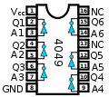
The 7404 hex inverter is a TTL chip with 14 pins. Two pins are used for VDD and GND, the other 12 pins are used for the 6 independent inverters. Both chips implement the expression \( Q_n = \overline A_n \) where each circuit functions as an independent inverter. The 4049 is a CMOS Hex Inverting Buffer with 16 pins. Two pins are used for VDD and GND, 12 pins are used for the 6 independent inverters. Pins 13 and 16 are not connected.


