| Buffer Gate | ||||||||||||||||||
| ANSI Symbol | ||||||||||||||||||
| Functional | ||||||||||||||||||
| Truth Table | ||||||||||||||||||
| ||||||||||||||||||
| ||||||||||||||||||
|
A buffer, is a basic logic gate that passes its input, unchanged, to its output. Its behavior is the opposite of a NOT gate. The main purpose of a buffer is to regenerate the input, usually using a strong high and a strong low. A buffer has one input and one output; its output always equals its input. Buffers are also used to increase the propagation delay of circuits by driving the large capacitive loads.
Contents
Description[edit]
| This section requires expansion; you can help adding the missing info. |
A buffer is a very basic active device that generates an output identical to its input. In most technologies, a buffer is made of two inverters back-to-back. One of the many purposes for a buffer is to regenerate weak output from non-restoring logic.
Design[edit]
| This section is empty; you can help add the missing info by editing this page. |
Symbolic representation[edit]
Buffers are typically drawn on schematics using one of a standard symbol. Below are three of the commonly found standard symbols.
| ANSI | IEC | DIN | British |
|---|---|---|---|
 |
|
 |

|
Implementations[edit]
A buffer can be implemented in variety of of technologies.
CMOS[edit]
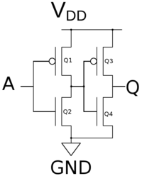
A CMOS buffer gate with one input and one output can be realized as simply two inverters back to back - built out of just 4 gates.
The table on the right shows the states of the four transistors with the various inputs of A.
| Buffer Gate by Transistor | |||||
|---|---|---|---|---|---|
| A | Q1 | Q2 | Q3 | Q4 | Q |
| 0 | 1 | 0 | 0 | 1 | 0 |
| 1 | 0 | 1 | 1 | 0 | 1 |
Discrete Chips[edit]
Various buffers/drivers exist chips as well for both 7400 series and 4000 series.
7400 series chips[edit]
| This section is empty; you can help add the missing info by editing this page. |
4000 series chips[edit]
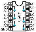
-CD4050 NonInverting 6 Channel (THE Jellybean go-to part for many people. This is often used as a 5 volt to 3.3 volt, voltage level shifter in hobby electronics for displays and sensors)
-CD4049 Inverting version of the CD4050.
-HEF40244 NonInverting 8 channel with 2 independently selected (4 channels each) tristate enable lines. This IC also has the advantage of inputs and outputs on opposing sides of the chip pin for pin.
The 7407 is a TTL chip with 14 pins. Two pins are used for VDD and GND, the other 12 pins are used for the 6 independent buffers. The 4050 is a CMOS Hex Buffer with 16 pins. Two pins are used for VDD and GND, 12 pins are used for the 6 independent buffers. Pins 13 and 16 are not connected. Both chips implement the expression QN = AN


