(added phone to list) |
|||
| Line 188: | Line 188: | ||
* [[used by::Nubia Red Magic 5G]] | * [[used by::Nubia Red Magic 5G]] | ||
* [[used by::Redmi K30 pro/pro zoom]] | * [[used by::Redmi K30 pro/pro zoom]] | ||
| + | * [[used by::Realme X50 Pro]] | ||
{{expand list}} | {{expand list}} | ||
== Documents == | == Documents == | ||
* [[:File:qualcomm-snapdragon-865-5g-mobile-platform-product-brief.pdf|Product Brief]] | * [[:File:qualcomm-snapdragon-865-5g-mobile-platform-product-brief.pdf|Product Brief]] | ||
Revision as of 19:10, 11 April 2020
| Edit Values | |
| Snapdragon 865 | |
 | |
| General Info | |
| Designer | Qualcomm, ARM Holdings |
| Manufacturer | TSMC |
| Model Number | SDM865 |
| Part Number | SM8250 |
| Market | Mobile |
| Introduction | December 4, 2019 (announced) March, 2020 (launched) |
| General Specs | |
| Family | Snapdragon 800 |
| Series | 800 |
| Frequency | 1,800 MHz, 2,420 MHz, 2,840 MHz |
| Microarchitecture | |
| ISA | ARMv8 (ARM) |
| Microarchitecture | Cortex-A77, Cortex-A55 |
| Core Name | Kryo 585 Gold, Kryo 585 Silver |
| Process | 7 nm |
| Technology | CMOS |
| Word Size | 64 bit |
| Cores | 8 |
| Threads | 8 |
| Max Memory | 16 GiB |
| Multiprocessing | |
| Max SMP | 1-Way (Uniprocessor) |
| Packaging | |
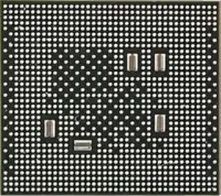 | |
| Succession | |
Snapdragon 865 is a high-performance 64-bit ARM system on a chip designed by Qualcomm and introduced in late 2019. Fabricated on TSMC's advanced 7nm (N7P) process, the 865 features four Kryo 585 Silver high-efficiency cores operating at 1.8 GHz along with three high-performance Kryo 585 Gold operating at 2.42 GHz and another prime Kryo 585 Gold core operating at 2.84 GHz. The Snapdragon 865 integrates the Adreno 650 GPU operation at 600 MHz and supports up to 16 GiB of quad-channel LPDDR5-5500 memory.
The Snapdragon 865 is designed to be paired with Qualcomm's 2nd generation 5G modem, the Snapdragon X55 5G modem (an external 7nm baseband chip produced by TSMC) and an RF front-end interface chip (RFFE) to bring 5G NR, sub-6 GHz and mmWave, support.
Contents
Cache
- Main articles: Cortex-A77 § Cache and Cortex-A55 § Cache
Prime Cortex-A77:
|
Cache Organization
Cache is a hardware component containing a relatively small and extremely fast memory designed to speed up the performance of a CPU by preparing ahead of time the data it needs to read from a relatively slower medium such as main memory. The organization and amount of cache can have a large impact on the performance, power consumption, die size, and consequently cost of the IC. Cache is specified by its size, number of sets, associativity, block size, sub-block size, and fetch and write-back policies. Note: All units are in kibibytes and mebibytes. |
|||||||||||||||||||||||||
|
|||||||||||||||||||||||||
3 core cluster Cortex-A77:
|
Cache Organization
Cache is a hardware component containing a relatively small and extremely fast memory designed to speed up the performance of a CPU by preparing ahead of time the data it needs to read from a relatively slower medium such as main memory. The organization and amount of cache can have a large impact on the performance, power consumption, die size, and consequently cost of the IC. Cache is specified by its size, number of sets, associativity, block size, sub-block size, and fetch and write-back policies. Note: All units are in kibibytes and mebibytes. |
|||||||||||||||||||||||||
|
|||||||||||||||||||||||||
Quad-core cluster Cortex-A55:
|
Cache Organization
Cache is a hardware component containing a relatively small and extremely fast memory designed to speed up the performance of a CPU by preparing ahead of time the data it needs to read from a relatively slower medium such as main memory. The organization and amount of cache can have a large impact on the performance, power consumption, die size, and consequently cost of the IC. Cache is specified by its size, number of sets, associativity, block size, sub-block size, and fetch and write-back policies. Note: All units are in kibibytes and mebibytes. |
|||||||||||||||||||||||||
|
|||||||||||||||||||||||||
- 4 MiB L3
Memory controller
|
Integrated Memory Controller
|
||||||||||||||||||
|
||||||||||||||||||
DSP
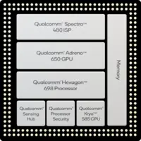
This chip features Qualcomm's Hexagon 698 DSP.
Graphics
|
Integrated Graphics Information
|
||||||||||||||||||||||||||||
|
||||||||||||||||||||||||||||
- Codec: H.265 (HEVC), H.264 (AVC), HDR10, HDR10+, HLG, VP8, VP9
- HDR Playback Codec support for HDR10+, HDR10, HLG and Dolby Vision
- Volumetric VR video playback
- 8K 360 VR video playback
Camera
- ISP
- Qualcomm Spectra 480 image signal processor
- Dual 14-bit CV-ISPs
- Hardware accelerator for computer vision (CV-ISP)
- ZSL
- Up to 30 MP dual camera
- Up to 64 MP single camera
- 200 MP Single
- Qualcomm Spectra 480 image signal processor
- Photo Capture: HEIF photo capture
- Video Capture:
- Dolby Vision, HDR10, HDR10+, HEVC
- 4K video capture with simultaneous 64 MP photo capture
- Rec. 2020 color gamut video capture
- Up to 10-bit color depth video capture
- Slow motion video capture up to 720p at 960fps, HEVC Video Capture
Connectivity
- From the FastConnect 6800 Module
- Wi-Fi
- Standards: 802.11ax, 802.11ac wave 2, 802.11a/b/g, 802.11n
- Bands: 2.4 GHz, 5 GHz
- Peak Speed: 1.774 Gbps
- 1024 QAM, 8x8 Sounding, MU-MIMO, Dual-band simultaneous (DBS), OFDMA, Target Wake-up Time (TWT)
- Bluetooth
- Bluetooth 5.1
- Wi-Fi
Location
- Systems: GPS, GLONASS, Beidou, Galileo, QZSS, SBAS, Dual frequency GNSS
Utilizing devices
- Samsung Galaxy S20
- Samsung Galaxy S20+
- Samsung Galaxy S20 Ultra
- Xiaomi Mi 10
- Xiaomi Mi 10 Pro
- Oppo Find X2
- Oppo Find X2 Pro
- Nubia Red Magic 5G
- Redmi K30 pro/pro zoom
- Realme X50 Pro
This list is incomplete; you can help by expanding it.
Documents
- all microprocessor models
- microprocessor models by qualcomm
- microprocessor models by qualcomm based on cortex-a77
- microprocessor models by qualcomm based on cortex-a55
- microprocessor models by arm holdings
- microprocessor models by arm holdings based on cortex-a77
- microprocessor models by arm holdings based on cortex-a55
- microprocessor models by tsmc
| Used by | Asus ROG 3 + and Asus ZENFONE 7 / 7 PRO + |
| back image | 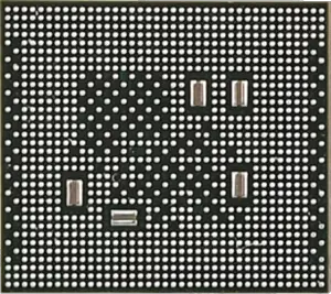 + + |
| base frequency | 2,420 MHz (2.42 GHz, 2,420,000 kHz) +, 2,840 MHz (2.84 GHz, 2,840,000 kHz) + and 2,110 MHz (2.11 GHz, 2,110,000 kHz) + |
| clock multiplier | 28 + |
| core count | 8 + |
| core name | Kryo 585 Gold +, Kryo 585 Silver + and kryo 585 prime + |
| core voltage (max) | 0.944 V (9.44 dV, 94.4 cV, 944 mV) + |
| core voltage (min) | 0.45 V (4.5 dV, 45 cV, 450 mV) + |
| designer | Qualcomm + and ARM Holdings + |
| dsp | Hexagon 698 DSP + |
| family | Snapdragon 800 + |
| first announced | December 4, 2019 + |
| first launched | March 2020 + |
| full page name | qualcomm/snapdragon 800/865 + |
| has ecc memory support | true + |
| has locked clock multiplier | false + |
| instance of | microprocessor + |
| integrated gpu | Adreno 650 GPU + |
| integrated gpu base frequency | 257 MHz (0.257 GHz, 257,000 KHz) + |
| integrated gpu designer | Qualcomm + |
| integrated gpu max frequency | 1,450 MHz (1.45 GHz, 1,450,000 KHz) + |
| isa | ARMv8 + |
| isa family | ARM + |
| l1$ size | 128 KiB (131,072 B, 0.125 MiB) +, 384 KiB (393,216 B, 0.375 MiB) + and 512 KiB (524,288 B, 0.5 MiB) + |
| l1d$ description | 4-way set associative + |
| l1d$ size | 64 KiB (65,536 B, 0.0625 MiB) +, 192 KiB (196,608 B, 0.188 MiB) + and 256 KiB (262,144 B, 0.25 MiB) + |
| l1i$ description | 4-way set associative + and 2-way set associative + |
| l1i$ size | 64 KiB (65,536 B, 0.0625 MiB) +, 192 KiB (196,608 B, 0.188 MiB) + and 256 KiB (262,144 B, 0.25 MiB) + |
| l2$ description | 8-way set associative + |
| l2$ size | 0.5 MiB (512 KiB, 524,288 B, 4.882812e-4 GiB) + and 0.75 MiB (768 KiB, 786,432 B, 7.324219e-4 GiB) + |
| ldate | 3000 + |
| main image |  + + |
| manufacturer | TSMC + |
| market segment | Mobile + |
| max cpu count | 1 + |
| max memory | 16,384 MiB (16,777,216 KiB, 17,179,869,184 B, 16 GiB, 0.0156 TiB) + |
| max memory bandwidth | 40.98 GiB/s (41,963.52 MiB/s, 44.002 GB/s, 44,001.94 MB/s, 0.04 TiB/s, 0.044 TB/s) + |
| max memory channels | 4 + |
| microarchitecture | Cortex-A77 + and Cortex-A55 + |
| model number | SDM865 + |
| name | Snapdragon 865 + |
| neuron count | 200,000 + |
| part number | SM8250 + |
| process | 7 nm (0.007 μm, 7.0e-6 mm) + |
| series | 800 + |
| smp max ways | 1 + |
| synapse count | 150,000 + |
| tdp | 10 W (10,000 mW, 0.0134 hp, 0.01 kW) + |
| tdp down | 3 W (3,000 mW, 0.00402 hp, 0.003 kW) + |
| tdp down frequency | 1,100 MHz (1.1 GHz, 1,100,000 kHz) + |
| tdp up | 10 W (10,000 mW, 0.0134 hp, 0.01 kW) + |
| tdp up frequency | 2,840 MHz (2.84 GHz, 2,840,000 kHz) + |
| technology | CMOS + |
| thread count | 8 + |
| used by | Samsung Galaxy S20 +, Samsung Galaxy S20+ +, Samsung Galaxy S20 Ultra +, Oppo Find X2 +, Oppo Find X2 Pro +, Nubia Red Magic 5G +, Xiaomi Black shark 3 +, Xiaomi Black shark 3 Pro +, Vivo IQOO 3 +, Vivo IQOO neo 3 +, ZTE Axon 10s Pro +, LG V60 ThinQ 5G UW +, LG V60 ThinQ 5G +, Meizu 17 +, Meizu 17 Pro +, Oppo Ace 2 +, Motorola Edge+ +, Vivo NEX 3S 5G +, Sony Xperia 1 II +, Vivo X50 Pro+ +, Xiaomi Mi 10 5G +, Xiaomi Mi 10 Pro 5G +, Realme X50 Pro 5G +, OnePlus 8 5G +, OnePlus 8 Pro 5G +, Samsung Galaxy Note 20 +, Samsung Galaxy Note 20 Ultra +, Samsung Galaxy S20 FE 5G +, OnePlus 8T 5G +, Nubia Red Magic 5S +, Redmi K30 pro +, Redmi K30 pro zoom +, Redmi K30S +, Realme X50 Pro Player +, Xiaomi Mi 10 Ultra +, Xiaomi Mi 10T 5G +, Xiaomi Mi 10T Pro 5G +, Xiaomi Black shark 3S +, Vivo IQOO 5 5G +, Vivo IQOO 5 Pro 5G +, Sony Xperia 5 II +, Xiaomi Poco F2 Pro 5G +, Poco F2 Pro +, Samsung Galaxy S20 FE 4G +, Samsung Galaxy Tab S7 +, Samsung Galaxy Tab S7+ + and Oppo Find X3 Neo + |
| word size | 64 bit (8 octets, 16 nibbles) + |
