(→Architecture) |
(mem setup) |
||
| Line 73: | Line 73: | ||
=== Block Diagram === | === Block Diagram === | ||
[[File:skylake block diagram.svg]] | [[File:skylake block diagram.svg]] | ||
| + | |||
| + | === Memory Hierarchy === | ||
| + | Other than a few organizational changes (e.g. L2$ went from 8-way to 4-way set associative), the overall memory structure is identical to {{\\|Broadwell}}/{{\\|Haswell}}. | ||
| + | * Cache | ||
| + | ** L1I Cache: | ||
| + | *** 32 KB 8-way set associative | ||
| + | **** 64 B line size | ||
| + | **** Write-back policy | ||
| + | **** shared by the two threads, per core | ||
| + | ** L1D Cache: | ||
| + | *** 32 KB 8-way set associative | ||
| + | *** 64 B line size | ||
| + | *** shared by the two threads, per core | ||
| + | *** 4 cycles for fastest load-to-use | ||
| + | *** 64 Bytes/cycle load bandwidth | ||
| + | *** 32 Bytes/cycle store bandwidth | ||
| + | *** Write-back policy | ||
| + | ** L2 Cache: | ||
| + | *** unified, 256 KB 4-way set associative | ||
| + | *** 12 cycles for fastest load-to-use | ||
| + | *** 64B/cycle bandwidth to L1$ | ||
| + | *** Write-back policy | ||
| + | ** L3 Cache: | ||
| + | *** Up to 2 MB | ||
| + | *** Per core | ||
| + | *** Up to 16-way set associative | ||
| + | *** Write-back policy | ||
| + | ** L4 Cache: | ||
| + | *** 128 MB | ||
| + | *** Per package | ||
| + | *** Only on the Iris Pro GPUs | ||
Revision as of 10:23, 2 May 2016
| Edit Values | |
| Skylake µarch | |
| General Info |
Skylake (SKL) is Intel's microarchitecture using 14 nm process for mainstream desktops, servers, and mobiles. Skylake became the successor to the short-lived Broadwell which experienced severe delays.
For desktop and mobile, Skylake is branded as 6th Generation Intel Core processors. For server class processors, Intel branded it as Xeon E3 v5, Xeon E5 v5, and Xeon E7 v5.
Contents
Codenames
| Core | Abbrev | Target |
|---|---|---|
| Skylake Y | SKL-Y | 2-in-1s detachable, tablets, and computer sticks |
| Skylake U | SKL-U | Light notebooks, portable All-in-Ones (AiOs), Minis, and conference room |
| Skylake H | SKL-H | Ultimate mobile performance, mobile workstations |
| Skylake S | SKL-S | Desktop performance to value, AiOs, and minis |
Technology
- Main article: Broadwell § Technology
Skylake uses the same 14 nm process used for the Broadwell microarchitecture.
Architecture
Overall Skylake builds upon Intel's previous microarchitecture, Broadwell, but includes a more beefed up front end, more optimized execution engine, and numerous number of smaller enhancements including
Key changes from Broadwell
- Front End
- Larger legacy pipeline delivery (5 µOPs, up from 4)
- Larger IDQ delivery (6 µOPs, up from 4)
- 2.28x larger allocation queue (64/thread, up from 28/thread)
- Improved branch prediction unit
- Execution Engine
- Larger re-order buffer (224 entries, up from 192)
- Larger scheduler (97 entries, up from 60)
- Larger Integer Register File (180 entries, up from 160)
- Larger store buffer (56 entries, up from 42)
- Memory
- L2$ was changed from 8-way to 4-way set associative
- TLBs
- ITLB
- 4KB page translations was changed from 4-way to 8-way associative
- STLB
- 4KB+2M page translations was changed from 6-way to 12-way associative
- ITLB
Graphics
- Skylake retires VGA support, multi-monitor support for up to 3 displays via HDMI 1.4, DP 1.2, and eDP 1.3 interfaces.
- Direct X 12
- OpenCL 2.0
- OpenGL 4.4
- Up to 24 EUs (same as Haswell, 48 EUs on Iris Pro Graphics)
New instructions
- Main article: See §Added_instructions for the complete list
Skylake introduced a number of new instructions:
-
SGX- Software Guard Extensions -
MPX-Memory Protection Extensions -
AVX-512- Advanced Vector Extensions 512
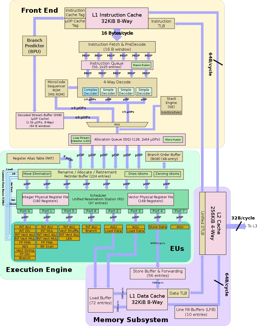
Block Diagram
Memory Hierarchy
Other than a few organizational changes (e.g. L2$ went from 8-way to 4-way set associative), the overall memory structure is identical to Broadwell/Haswell.
- Cache
- L1I Cache:
- 32 KB 8-way set associative
- 64 B line size
- Write-back policy
- shared by the two threads, per core
- 32 KB 8-way set associative
- L1D Cache:
- 32 KB 8-way set associative
- 64 B line size
- shared by the two threads, per core
- 4 cycles for fastest load-to-use
- 64 Bytes/cycle load bandwidth
- 32 Bytes/cycle store bandwidth
- Write-back policy
- L2 Cache:
- unified, 256 KB 4-way set associative
- 12 cycles for fastest load-to-use
- 64B/cycle bandwidth to L1$
- Write-back policy
- L3 Cache:
- Up to 2 MB
- Per core
- Up to 16-way set associative
- Write-back policy
- L4 Cache:
- 128 MB
- Per package
- Only on the Iris Pro GPUs
- L1I Cache:
