(→Die size) |
(→Known good die) |
||
| (5 intermediate revisions by 2 users not shown) | |||
| Line 5: | Line 5: | ||
== Overview == | == Overview == | ||
| − | The die is the final product of the [[fabrication process]]. A fully processed wafer will | + | The '''die''' is the final product of the [[fabrication process]]. A fully processed wafer will undergo [[singulation]] following [[wafer probing|probing]]. Depending on the application, the die may be shipped to an assembly/packaging plant where it will undergo further [[encapsulation]], producing the final chip that ships to customers. |
=== Known good die === | === Known good die === | ||
{{main|known good die|l1=Known Good Die (KGD)}} | {{main|known good die|l1=Known Good Die (KGD)}} | ||
| − | A '''[[known good die]]''' is a special type of bare die that underwent additional testing and screening post-[[singulation]]. KGD testing ensures the die meets the required specification prior to getting packaged. KGDs are especially important in [[multi-chip packages]] where multiple dies in a single package must function correctly to produce the required product. | + | A '''[[known good die]]''' ('''KGD''') is a special type of bare die that underwent additional testing and screening post-[[singulation]]. KGD testing ensures the die meets the required specification prior to getting packaged. KGDs are especially important in [[multi-chip packages]] where multiple dies in a single package must function correctly to produce the required product. |
== Die size == | == Die size == | ||
| + | {{main|die size}} | ||
Die size refers to the length and width of the die. Since the die size and shape determines the total number of dies that may be realized from a single [[wafer]], the die size is a strong indicator of cost. | Die size refers to the length and width of the die. Since the die size and shape determines the total number of dies that may be realized from a single [[wafer]], the die size is a strong indicator of cost. | ||
| Line 20: | Line 21: | ||
|- style="vertical-align: top;" | |- style="vertical-align: top;" | ||
| | | | ||
| + | * 826 mm² (GA100) | ||
* 815 mm² (GV100) | * 815 mm² (GV100) | ||
* 754 mm² (TU102) | * 754 mm² (TU102) | ||
| + | * 628 mm² (GA102) | ||
* 610 mm² (GP100) | * 610 mm² (GP100) | ||
* 601 mm² (GM200) | * 601 mm² (GM200) | ||
* 596 mm² (Fiji) | * 596 mm² (Fiji) | ||
* 576 mm² (GT200) | * 576 mm² (GT200) | ||
| − | * | + | * 561 mm² (GK110) |
* 545 mm² (TU104) | * 545 mm² (TU104) | ||
* 510 mm² (Vega 10) | * 510 mm² (Vega 10) | ||
Latest revision as of 08:08, 21 February 2023


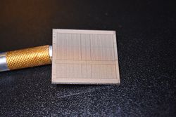
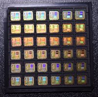
A die is the actual bare IC chip and is the final product of the fabrication process. It is the individual chip made following the singulation of a wafer. Dies typically undergo packaging before being sold to the customer as a final product.
Contents
Overview[edit]
The die is the final product of the fabrication process. A fully processed wafer will undergo singulation following probing. Depending on the application, the die may be shipped to an assembly/packaging plant where it will undergo further encapsulation, producing the final chip that ships to customers.
Known good die[edit]
- Main article: Known Good Die (KGD)
A known good die (KGD) is a special type of bare die that underwent additional testing and screening post-singulation. KGD testing ensures the die meets the required specification prior to getting packaged. KGDs are especially important in multi-chip packages where multiple dies in a single package must function correctly to produce the required product.
Die size[edit]
- Main article: die size
Die size refers to the length and width of the die. Since the die size and shape determines the total number of dies that may be realized from a single wafer, the die size is a strong indicator of cost.
| Select Large Dies | |||
|---|---|---|---|
| GPU | Server | Desktop | Mobile |
|
|
|
|
This list is incomplete; you can help by expanding it.