From WikiChip
Difference between revisions of "nvidia/microarchitectures/carmel"
(→Performance claims: single core result, not rate) |
|||
| (10 intermediate revisions by one other user not shown) | |||
| Line 9: | Line 9: | ||
|cores=8 | |cores=8 | ||
|type=Superscalar | |type=Superscalar | ||
| − | |||
| − | |||
| − | |||
| − | |||
|isa=ARMv8 | |isa=ARMv8 | ||
|feature=RAS | |feature=RAS | ||
| Line 19: | Line 15: | ||
|l3=4 MiB | |l3=4 MiB | ||
|l3 per=complex | |l3 per=complex | ||
| − | |predecessor= | + | |predecessor=Denver 2 |
| − | |predecessor link= | + | |predecessor link=nvidia/microarchitectures/denver 2 |
}} | }} | ||
| + | '''Carmel''' is a the successor to {{\\|Denver 2}}, an [[ARM]] microarchitecture for [[Nvidia]]'s {{nvidia|Tegra}} series of [[SoCs]]. | ||
| + | |||
| + | == Process Technology == | ||
| + | Carmel is integrated into chips fabricated on [[TSMC]] [[12 nm process]] (12FFN) | ||
| + | |||
| + | == Architecture == | ||
| + | Nvidia disclosed very few details regarding Carmel. Carmel is a 10-wide superscalar with each core supporting dual execution mode. | ||
| + | |||
| + | === Key changes from {{\\|Denver 2}} === | ||
| + | * [[12 nm]] (12FFN) | ||
| + | * ARMv8.2 | ||
| + | ** ARM RAS standard support | ||
| + | * Wider dispatch (10, up from 7) | ||
| + | |||
| + | === Memory Hierarchy === | ||
| + | * Cache | ||
| + | ** Parity & ECC | ||
| + | ** L1 | ||
| + | ** L2 | ||
| + | *** 2 MiB | ||
| + | **** Shared per duplex | ||
| + | ** L3 | ||
| + | *** 4 MiB | ||
| + | **** Shared by entire cluster | ||
| + | **** Exclusive | ||
| + | |||
| + | === Block Diagram === | ||
| + | ==== CPU Complex ==== | ||
| + | [[File:nvidia carmel complex diagram.svg|600px]] | ||
| + | |||
| + | == Overview == | ||
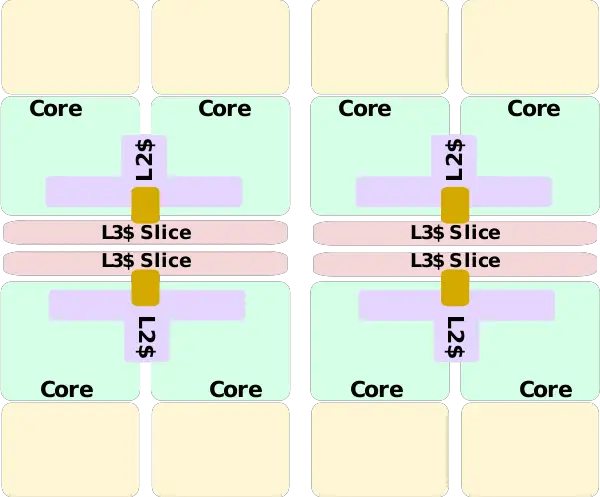
| + | Carmel is a CPU microarchitecture designed by Nvidia for their SoCs. The design consists of an 8-core cluster made of 4 core duplexes. The entire complex has [[cache coherency]] as well as an I/O coherent memory subsystem which is designed for communication with the various other accelerators on their SoCs such as the vision accelerator, deep learning accelerator, multimedia engine, and the GPU. | ||
| + | |||
| + | The cores consume 500-1,500 mW per core. | ||
| + | |||
| + | === Performance claims === | ||
| + | {| class="wikitable" | ||
| + | |- | ||
| + | ! SPECint 2000 Rate !! SPECint 2006 | ||
| + | |- | ||
| + | | 2700 || 21 | ||
| + | |} | ||
| + | |||
| + | == Die == | ||
| + | === CPU Complex === | ||
| + | * 8 cores | ||
| + | ** 4 duplexes | ||
| + | ** shared L3 | ||
| + | * ~62.25 mm² die size area | ||
| + | |||
| + | :[[File:nvidia carmel complex.png|class=wikichip_ogimage|600px]] | ||
| + | |||
| + | |||
| + | :[[File:nvidia carmel complex (annotated).png|600px]] | ||
| + | |||
| + | === CPU Duplex === | ||
| + | * 2 cores | ||
| + | * ~11.4 mm² die size area | ||
| + | |||
| + | :[[File:nvidia carmel duplex.png|400px]] | ||
| + | |||
| + | |||
| + | :[[File:nvidia carmel duplex (annotated).png|400px]] | ||
| + | |||
| + | === Core === | ||
| + | * ~5.75 mm² die size area | ||
| + | |||
| + | :[[File:nvidia carmel core.png|200px]] | ||
| + | |||
| + | == Bibliography == | ||
| + | * IEEE Hot Chips 30 Symposium (HCS) 2018. | ||
Latest revision as of 10:27, 30 April 2019
| Edit Values | |
| Carmel µarch | |
| General Info | |
| Arch Type | CPU |
| Designer | Nvidia |
| Manufacturer | TSMC |
| Introduction | January 7, 2018 |
| Process | 12 nm |
| Core Configs | 8 |
| Pipeline | |
| Type | Superscalar |
| Instructions | |
| ISA | ARMv8 |
| Cache | |
| L2 Cache | 2 MiB/cluster |
| L3 Cache | 4 MiB/complex |
| Succession | |
Carmel is a the successor to Denver 2, an ARM microarchitecture for Nvidia's Tegra series of SoCs.
Contents
Process Technology[edit]
Carmel is integrated into chips fabricated on TSMC 12 nm process (12FFN)
Architecture[edit]
Nvidia disclosed very few details regarding Carmel. Carmel is a 10-wide superscalar with each core supporting dual execution mode.
Key changes from Denver 2[edit]
- 12 nm (12FFN)
- ARMv8.2
- ARM RAS standard support
- Wider dispatch (10, up from 7)
Memory Hierarchy[edit]
- Cache
- Parity & ECC
- L1
- L2
- 2 MiB
- Shared per duplex
- 2 MiB
- L3
- 4 MiB
- Shared by entire cluster
- Exclusive
- 4 MiB
Block Diagram[edit]
CPU Complex[edit]
Overview[edit]
Carmel is a CPU microarchitecture designed by Nvidia for their SoCs. The design consists of an 8-core cluster made of 4 core duplexes. The entire complex has cache coherency as well as an I/O coherent memory subsystem which is designed for communication with the various other accelerators on their SoCs such as the vision accelerator, deep learning accelerator, multimedia engine, and the GPU.
The cores consume 500-1,500 mW per core.
Performance claims[edit]
| SPECint 2000 Rate | SPECint 2006 |
|---|---|
| 2700 | 21 |
Die[edit]
CPU Complex[edit]
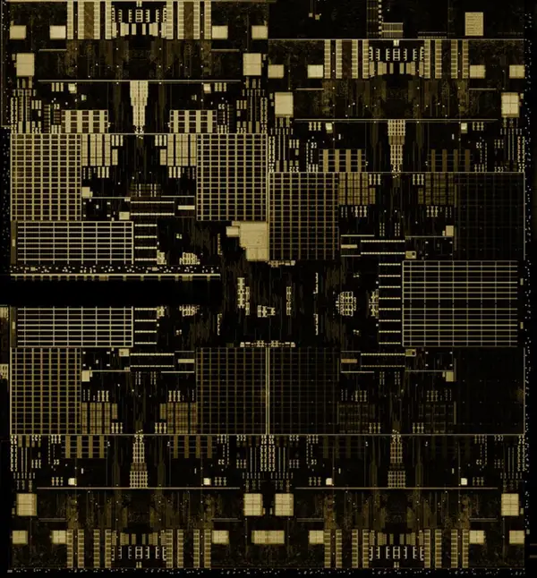
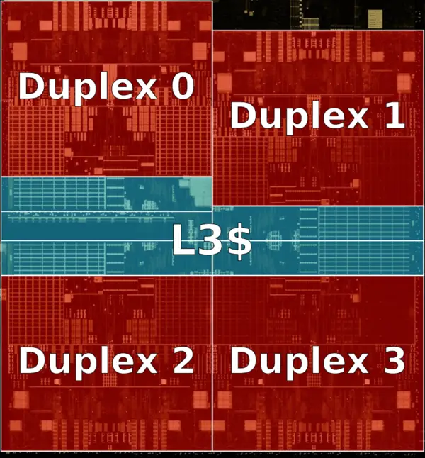
- 8 cores
- 4 duplexes
- shared L3
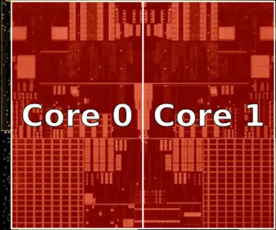
- ~62.25 mm² die size area
CPU Duplex[edit]
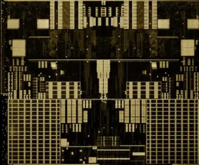
- 2 cores
- ~11.4 mm² die size area
Core[edit]
- ~5.75 mm² die size area
Bibliography[edit]
- IEEE Hot Chips 30 Symposium (HCS) 2018.
Facts about "Carmel - Microarchitectures - Nvidia"
| codename | Carmel + |
| core count | 8 + |
| designer | Nvidia + |
| first launched | January 7, 2018 + |
| full page name | nvidia/microarchitectures/carmel + |
| instance of | microarchitecture + |
| instruction set architecture | ARMv8 + |
| manufacturer | TSMC + |
| microarchitecture type | CPU + |
| name | Carmel + |
| process | 12 nm (0.012 μm, 1.2e-5 mm) + |
