From WikiChip
Difference between revisions of "renesas/r-car/h1"
m (Bot: moving all {{mpu}} to {{chip}}) |
|||
| (18 intermediate revisions by one other user not shown) | |||
| Line 1: | Line 1: | ||
{{renesas title|R-Car H1}} | {{renesas title|R-Car H1}} | ||
| − | {{ | + | {{chip |
|name=R-Car H1 | |name=R-Car H1 | ||
|image=r-car h1.png | |image=r-car h1.png | ||
| Line 8: | Line 8: | ||
|model number=H1 | |model number=H1 | ||
|part number=R8A77790 | |part number=R8A77790 | ||
| + | |market=Embedded | ||
|first announced=October 21, 2011 | |first announced=October 21, 2011 | ||
|first launched=November, 2011 | |first launched=November, 2011 | ||
|family=R-Car | |family=R-Car | ||
| − | |series= | + | |series=1st Gen |
|frequency=800 MHz | |frequency=800 MHz | ||
|frequency 2=1000 MHz | |frequency 2=1000 MHz | ||
| Line 18: | Line 19: | ||
|microarch=Cortex-A9 | |microarch=Cortex-A9 | ||
|microarch 2=SH-4A | |microarch 2=SH-4A | ||
| + | |core name=Cortex-A9 | ||
| + | |core name 2=SH-4A | ||
|process=40 nm | |process=40 nm | ||
|technology=CMOS | |technology=CMOS | ||
| Line 29: | Line 32: | ||
|package module 1={{packages/renesas/fcbga-832}} | |package module 1={{packages/renesas/fcbga-832}} | ||
}} | }} | ||
| − | '''R-Car H1''' is a high-end embedded [[penta-core]] SoC for the automotive industry designed by [[Renesas]] and introduced in 2011 | + | '''R-Car H1''' is a high-end embedded [[penta-core]] SoC for the automotive industry designed by [[Renesas]] and introduced in 2011. The H1 features [[5 cores]], four {{armh|Cortex-A9|l=arch}} cores operating at 1 GHz and an additional {{renesas|SH-4A|l=arch}} core operating at 800 MHz intended for real-time processing multimedia engine (MME). This chip incorporates [[Imagination]]'s {{imgtec|PowerVR SGX543}}-MP2 [[GPU]]. The H1 supports up to 2 GiB of dual-channel DDR3-1066 memory. |
| + | |||
| + | Announced in late 2011, Renesas expected mass production begin in December 2012 with a peak rate of 100,000 units per month by December 2013. | ||
== Cache == | == Cache == | ||
| Line 37: | Line 42: | ||
|l1i cache=128 KiB | |l1i cache=128 KiB | ||
|l1i break=4x32 KiB | |l1i break=4x32 KiB | ||
| + | |l1i desc=4-way set associative | ||
|l1d cache=128 KiB | |l1d cache=128 KiB | ||
|l1d break=4x32 KiB | |l1d break=4x32 KiB | ||
| + | |l1d desc=4-way set associative | ||
|l2 cache=1 MiB | |l2 cache=1 MiB | ||
|l2 break=4x256 KiB | |l2 break=4x256 KiB | ||
| Line 80: | Line 87: | ||
== Graphics == | == Graphics == | ||
| + | * Display out × 2 ch (RGB888) | ||
| + | * Video input x 2 ch | ||
| + | * Video decode processor (H.264/AVC, MPEG-4, VC-1) | ||
{{integrated graphics | {{integrated graphics | ||
| gpu = PowerVR SGX543 | | gpu = PowerVR SGX543 | ||
| Line 86: | Line 96: | ||
| max displays = 2 | | max displays = 2 | ||
| frequency = 250 MHz | | frequency = 250 MHz | ||
| − | |||
| − | |||
| − | |||
| − | |||
| − | |||
| − | |||
| − | |||
| − | |||
| − | |||
| opengl es ver = 2.0 | | opengl es ver = 2.0 | ||
| Line 101: | Line 102: | ||
| directx = 9.0 L1 | | directx = 9.0 L1 | ||
}} | }} | ||
| + | |||
| + | == Audio == | ||
| + | * Sound processing unit × 2 ch | ||
| + | * Sampling rate converter × 10 ch | ||
| + | * Sound serial interface × 10 ch | ||
| + | * MOST DTCP | ||
| + | |||
| + | == Features == | ||
| + | {{arm features | ||
| + | |thumb=No | ||
| + | |thumb2=Yes | ||
| + | |thumbee=Yes | ||
| + | |vfpv1=No | ||
| + | |vfpv2=No | ||
| + | |vfpv3=Yes | ||
| + | |vfpv3-d16=No | ||
| + | |vfpv3-f16=No | ||
| + | |vfpv4=No | ||
| + | |vfpv4-d16=No | ||
| + | |vfpv5=No | ||
| + | |neon=Yes | ||
| + | |jazelle=Yes | ||
| + | |wmmx=No | ||
| + | |wmmx2=No | ||
| + | }} | ||
| + | |||
| + | == Block Diagram == | ||
| + | : [[File:rcar h1 block.png|650px]] | ||
| + | |||
| + | |||
| + | : [[File:r-car h1 block.png|650px]] | ||
| + | |||
| + | == Dev Board ("MARZEN") == | ||
| + | * 200 mmx 150 mm | ||
| + | * R-CAR H1 | ||
| + | * 64 MiB flash memory | ||
| + | * 1 MiB serial flash/E²PROM | ||
| + | * 2 x512 MiB DDR3-DRAM | ||
| + | * RS-232C, UART,USB, SD, LAN, SATA, PCI, CAN, and MLB interfaces | ||
| + | * Analog RGB with DSUB 15-pin and/or LVDS flat cable connector | ||
| + | * switches,LEDs, I/O expansion | ||
| + | |||
| + | : [[File:renesas marzen h1 board.png|450px]] | ||
Latest revision as of 15:32, 13 December 2017
| Edit Values | |||||||||||
| R-Car H1 | |||||||||||
 | |||||||||||
| General Info | |||||||||||
| Designer | Renesas, ARM Holdings | ||||||||||
| Manufacturer | TSMC | ||||||||||
| Model Number | H1 | ||||||||||
| Part Number | R8A77790 | ||||||||||
| Market | Embedded | ||||||||||
| Introduction | October 21, 2011 (announced) November, 2011 (launched) | ||||||||||
| General Specs | |||||||||||
| Family | R-Car | ||||||||||
| Series | 1st Gen | ||||||||||
| Frequency | 800 MHz, 1000 MHz | ||||||||||
| Microarchitecture | |||||||||||
| ISA | ARMv7 (ARM) | ||||||||||
| Microarchitecture | Cortex-A9, SH-4A | ||||||||||
| Core Name | Cortex-A9, SH-4A | ||||||||||
| Process | 40 nm | ||||||||||
| Technology | CMOS | ||||||||||
| Word Size | 32 bit | ||||||||||
| Cores | 5 | ||||||||||
| Threads | 5 | ||||||||||
| Max Memory | 2 GiB | ||||||||||
| Multiprocessing | |||||||||||
| Max SMP | 1-Way (Uniprocessor) | ||||||||||
| Electrical | |||||||||||
| Vcore | 1.2 V | ||||||||||
| VI/O | 3.3 V | ||||||||||
| Packaging | |||||||||||
| |||||||||||
R-Car H1 is a high-end embedded penta-core SoC for the automotive industry designed by Renesas and introduced in 2011. The H1 features 5 cores, four Cortex-A9 cores operating at 1 GHz and an additional SH-4A core operating at 800 MHz intended for real-time processing multimedia engine (MME). This chip incorporates Imagination's PowerVR SGX543-MP2 GPU. The H1 supports up to 2 GiB of dual-channel DDR3-1066 memory.
Announced in late 2011, Renesas expected mass production begin in December 2012 with a peak rate of 100,000 units per month by December 2013.
Contents
Cache[edit]
- Main article: Cortex-A9 § Cache
|
Cache Organization
Cache is a hardware component containing a relatively small and extremely fast memory designed to speed up the performance of a CPU by preparing ahead of time the data it needs to read from a relatively slower medium such as main memory. The organization and amount of cache can have a large impact on the performance, power consumption, die size, and consequently cost of the IC. Cache is specified by its size, number of sets, associativity, block size, sub-block size, and fetch and write-back policies. Note: All units are in kibibytes and mebibytes. |
|||||||||||||||||||||||||
|
|||||||||||||||||||||||||
Memory controller[edit]
|
Integrated Memory Controller
|
||||||||||||||||
|
||||||||||||||||
Expansions[edit]
|
Expansion Options
|
||||||||||||||||||||||||||||||||||
|
||||||||||||||||||||||||||||||||||
- 3 x HSPI
- MLB (MOST150) 6-Pin I/F
- 2 x CAN 32 Message Buffers
- MMC
- 4 x SD
Graphics[edit]
- Display out × 2 ch (RGB888)
- Video input x 2 ch
- Video decode processor (H.264/AVC, MPEG-4, VC-1)
|
Integrated Graphics Information
|
||||||||||||||||||||||||||
|
||||||||||||||||||||||||||
Audio[edit]
- Sound processing unit × 2 ch
- Sampling rate converter × 10 ch
- Sound serial interface × 10 ch
- MOST DTCP
Features[edit]
[Edit/Modify Supported Features]
|
Supported ARM Extensions & Processor Features
|
||||||||||
|
||||||||||
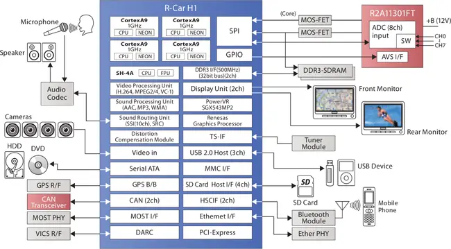
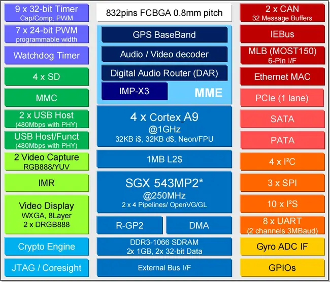
Block Diagram[edit]
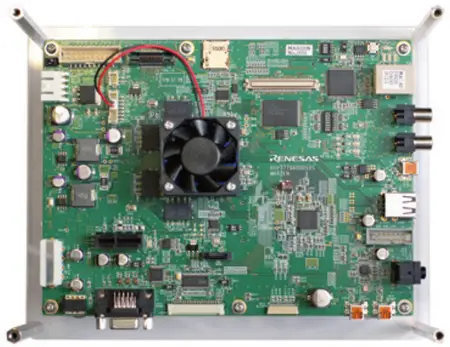
Dev Board ("MARZEN")[edit]
- 200 mmx 150 mm
- R-CAR H1
- 64 MiB flash memory
- 1 MiB serial flash/E²PROM
- 2 x512 MiB DDR3-DRAM
- RS-232C, UART,USB, SD, LAN, SATA, PCI, CAN, and MLB interfaces
- Analog RGB with DSUB 15-pin and/or LVDS flat cable connector
- switches,LEDs, I/O expansion
Categories:
- all microprocessor models
- microprocessor models by renesas
- microprocessor models by renesas based on cortex-a9
- microprocessor models by renesas based on sh-4a
- microprocessor models by arm holdings
- microprocessor models by arm holdings based on cortex-a9
- microprocessor models by arm holdings based on sh-4a
- microprocessor models by tsmc
Facts about "R-Car H1 - Renesas"
| Has subobject "Has subobject" is a predefined property representing a container construct and is provided by Semantic MediaWiki. | R-Car H1 - Renesas#package + and R-Car H1 - Renesas#io + |
| base frequency | 800 MHz (0.8 GHz, 800,000 kHz) + and 1,000 MHz (1 GHz, 1,000,000 kHz) + |
| core count | 5 + |
| core name | Cortex-A9 + and SH-4A + |
| core voltage | 1.2 V (12 dV, 120 cV, 1,200 mV) + |
| designer | Renesas + and ARM Holdings + |
| family | R-Car + |
| first announced | October 21, 2011 + |
| first launched | November 2011 + |
| full page name | renesas/r-car/h1 + |
| has ecc memory support | false + |
| instance of | microprocessor + |
| integrated gpu | PowerVR SGX543 + |
| integrated gpu base frequency | 250 MHz (0.25 GHz, 250,000 KHz) + |
| integrated gpu designer | Imagination Technologies + |
| integrated gpu execution units | 2 + |
| io voltage | 3.3 V (33 dV, 330 cV, 3,300 mV) + |
| isa | ARMv7 + |
| isa family | ARM + |
| l1$ size | 256 KiB (262,144 B, 0.25 MiB) + |
| l1d$ description | 4-way set associative + |
| l1d$ size | 128 KiB (131,072 B, 0.125 MiB) + |
| l1i$ description | 4-way set associative + |
| l1i$ size | 128 KiB (131,072 B, 0.125 MiB) + |
| l2$ size | 1 MiB (1,024 KiB, 1,048,576 B, 9.765625e-4 GiB) + |
| ldate | November 2011 + |
| main image | 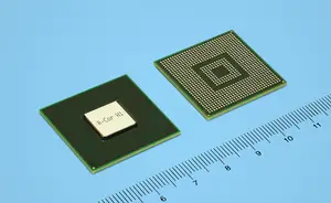 + + |
| manufacturer | TSMC + |
| market segment | Embedded + |
| max cpu count | 1 + |
| max memory | 2,048 MiB (2,097,152 KiB, 2,147,483,648 B, 2 GiB, 0.00195 TiB) + |
| max memory bandwidth | 7.95 GiB/s (8,140.8 MiB/s, 8.536 GB/s, 8,536.248 MB/s, 0.00776 TiB/s, 0.00854 TB/s) + |
| max memory channels | 2 + |
| max pcie lanes | 1 + |
| microarchitecture | Cortex-A9 + and SH-4A + |
| model number | H1 + |
| name | R-Car H1 + |
| package | FCBGA-832 + |
| part number | R8A77790 + |
| process | 40 nm (0.04 μm, 4.0e-5 mm) + |
| series | 1st Gen + |
| smp max ways | 1 + |
| supported memory type | DDR3-1066 + |
| technology | CMOS + |
| thread count | 5 + |
| word size | 32 bit (4 octets, 8 nibbles) + |
