Semiconductor & Computer Engineering
From WikiChip
Difference between revisions of "intel/atom x5/x5-e3930"
(Created page with "{{intel title|Atom x5-E3930}} {{mpu | name = Intel Atom x5-E3930 | no image = Yes | image = | image size = | caption...") |
|||
| (21 intermediate revisions by 3 users not shown) | |||
| Line 1: | Line 1: | ||
{{intel title|Atom x5-E3930}} | {{intel title|Atom x5-E3930}} | ||
| − | {{ | + | {{chip |
| name = Intel Atom x5-E3930 | | name = Intel Atom x5-E3930 | ||
| − | | no image = | + | | no image = |
| − | | image = | + | | image = Atom E3900 SoC Front.png |
| image size = | | image size = | ||
| caption = | | caption = | ||
| + | | designer = Intel | ||
| manufacturer = Intel | | manufacturer = Intel | ||
| model number = x5-E3930 | | model number = x5-E3930 | ||
| part number = | | part number = | ||
| − | | market = | + | | market = Embedded |
| first announced = October 26, 2016 | | first announced = October 26, 2016 | ||
| first launched = 2017 | | first launched = 2017 | ||
| Line 30: | Line 31: | ||
| cpuid = | | cpuid = | ||
| + | | isa family = x86 | ||
| + | | isa = x86-64 | ||
| microarch = Goldmont | | microarch = Goldmont | ||
| platform = Apollo Lake | | platform = Apollo Lake | ||
| Line 42: | Line 45: | ||
| thread count = 2 | | thread count = 2 | ||
| max cpus = 1 | | max cpus = 1 | ||
| − | | max memory = | + | | max memory = 8 GiB |
| max memory addr = | | max memory addr = | ||
| − | + | ||
| power = | | power = | ||
| − | | sdp = | + | | sdp = |
| − | | tdp = | + | | tdp = 6.5 W |
| ctdp down = | | ctdp down = | ||
| ctdp down frequency = | | ctdp down frequency = | ||
| ctdp up = | | ctdp up = | ||
| + | | tjunc min = -40 °C | ||
| + | | tjunc max = 110 °C | ||
| + | | tcase min = | ||
| + | | tcase max = | ||
| + | | tstorage min = | ||
| + | | tstorage max = | ||
| packaging = Yes | | packaging = Yes | ||
| Line 63: | Line 72: | ||
| socket 0 = BGA-1296 | | socket 0 = BGA-1296 | ||
| socket 0 type = BGA | | socket 0 type = BGA | ||
| + | }} | ||
| + | The '''Atom x5-E3930''' is a {{arch|64}} [[dual-core]] [[x86]] system on a chip set introduced by [[Intel]] in early 2017. This ultra-low power MPU, which was specifically designed for the [[internet of things|IoTs]], operates at 1.3 GHz and has a TDP of 6.5 W. This chip is based on the {{intel|Goldmont|l=arch}}, manufactured on Intel's enhanced [[14 nm process]]. | ||
| + | |||
| + | == Cache == | ||
| + | {{main|intel/microarchitectures/goldmont#Memory_Hierarchy|l1=Goldmont § Cache}} | ||
| + | {{cache info | ||
| + | |l1i cache=64 KiB | ||
| + | |l1i break=2x32 KiB | ||
| + | |l1i desc=8-way set associative | ||
| + | |l1i extra=(per core) | ||
| + | |l1d cache=48 KiB | ||
| + | |l1d break=2x24 KiB | ||
| + | |l1d desc=6-way set associative | ||
| + | |l1d extra=(per core) | ||
| + | |l2 cache=2 MiB | ||
| + | |l2 break=2x1 MiB | ||
| + | |l2 desc=16-way set associative | ||
| + | |l2 extra=(per 2 cores) | ||
| + | |l3 cache=0 KiB | ||
| + | |l3 desc=No L3$ | ||
| + | }} | ||
| + | |||
| + | == Memory controller == | ||
| + | {{integrated memory controller | ||
| + | | type = DDR3L-1866 | ||
| + | | type 2 = LPDDR4-2133 | ||
| + | | controllers = 1 | ||
| + | | channels = 4 | ||
| + | | ecc support = Yes | ||
| + | | max bandwidth = 31.79 GiB/s | ||
| + | | bandwidth schan = 15.89 GiB/s | ||
| + | | bandwidth dchan = 31.79 GiB/s | ||
| + | | max memory = 8 GiB | ||
| + | | pae = 40 bit | ||
| + | }} | ||
| + | |||
| + | == Graphics == | ||
| + | {{integrated graphic | ||
| + | | gpu = HD Graphics 500 | ||
| + | | device id = 0x5A85 | ||
| + | | execution units = 12 | ||
| + | | displays = 3 | ||
| + | | frequency = 400 MHz | ||
| + | | max frequency = 550 MHz | ||
| + | | max memory = 2 GiB | ||
| + | |||
| + | | output crt = | ||
| + | | output sdvo = | ||
| + | | output dsi = Yes | ||
| + | | output edp = Yes | ||
| + | | output dp = Yes | ||
| + | | output hdmi = Yes | ||
| + | | output vga = | ||
| + | | output dvi = | ||
| + | |||
| + | | directx ver = 12 | ||
| + | | opengl ver = 4.3 | ||
| + | | opencl ver = 1.2 | ||
| + | | opengl es ver = 3.0 | ||
| + | | hdmi ver = 1.4b | ||
| + | | dvi ver = | ||
| + | | dsi ver = | ||
| + | | vulkan ver = | ||
| + | | dp ver = 1.2 | ||
| + | | edp ver = 1.3 | ||
| + | |||
| + | | max res hdmi = 3840x2160 | ||
| + | | max res hdmi freq = 30 Hz | ||
| + | | max res dvi = | ||
| + | | max res dvi freq = | ||
| + | | max res dsi = 2560x1600 | ||
| + | | max res dsi freq = 60 Hz | ||
| + | | max res dp = 4096x2160 | ||
| + | | max res dp freq = 60 Hz | ||
| + | | max res edp = 3840x2160 | ||
| + | | max res edp freq = 60 Hz | ||
| + | | max res vga = | ||
| + | | max res vga freq = | ||
| + | |||
| + | | intel quick sync = Yes | ||
| + | | intel intru 3d = | ||
| + | | intel insider = | ||
| + | | intel widi = | ||
| + | | intel fdi = | ||
| + | | intel clear video = Yes | ||
| + | }} | ||
| + | |||
| + | * Video decode hardware acceleration including support for HEVC (H.265), H.264, MVC, VP8, VP9, MPEG2, VC-1, WMV9, JPEG/MJPEG. | ||
| + | * Video encode hardware acceleration including support for HEVC (H.265), H.264, MVC, VP8, VP9, JPEG/MJPEG. | ||
| + | |||
| + | == Expansions == | ||
| + | {{expansions | ||
| + | | pcie revision = 2.0 | ||
| + | | pcie lanes = 4 | ||
| + | | pcie config = 4x1 | ||
| + | | pcie config 1 = 1x4 + 1x2 | ||
| + | | pcie config 2 = 2x1 + 1x2 + 1x2 | ||
| + | | usb revision = 2.0 | ||
| + | | usb revision 2 = 3.0 | ||
| + | | usb ports = 6 | ||
| + | | sata revision = 3.0 | ||
| + | | sata ports = | ||
| + | | integrated lan = | ||
| + | | uart = Yes | ||
| + | | gp io = Yes | ||
| + | }} | ||
| + | |||
| + | == Features == | ||
| + | {{x86 features | ||
| + | | em64t = Yes | ||
| + | | nx = Yes | ||
| + | | txt = | ||
| + | | tsx = | ||
| + | | vpro = | ||
| + | | ht = | ||
| + | | tbt1 = | ||
| + | | tbt2 = | ||
| + | | bpt = Yes | ||
| + | | vt-x = Yes | ||
| + | | vt-d = Yes | ||
| + | | ept = Yes | ||
| + | | mmx = Yes | ||
| + | | sse = Yes | ||
| + | | sse2 = Yes | ||
| + | | sse3 = Yes | ||
| + | | ssse3 = Yes | ||
| + | | sse4.1 = Yes | ||
| + | | sse4.2 = Yes | ||
| + | | aes = Yes | ||
| + | | pclmul = Yes | ||
| + | | avx = | ||
| + | | avx2 = | ||
| + | | bmi = | ||
| + | | bmi1 = | ||
| + | | bmi2 = | ||
| + | | f16c = | ||
| + | | fma3 = | ||
| + | | mpx = | ||
| + | | sgx = | ||
| + | | eist = Yes | ||
| + | | secure key = Yes | ||
| + | | os guard = | ||
| + | | intel at = | ||
| + | | intel ipt = Yes | ||
}} | }} | ||
| + | == Die Shot == | ||
| + | Intel {{intel|Goldmont|l=arch}}-based {{intel|Atom}} E3900 SoC series die shot: | ||
| + | :[[File:atom e3900 die shot.jpg|650px]] | ||
| − | + | == Documents == | |
| + | * [[:File:atom-e3900-fact-sheet.pdf|Intel Atom Processor E3900 Series Fact Sheet]] | ||
Latest revision as of 04:09, 24 October 2019
| Edit Values | |
| Intel Atom x5-E3930 | |
 | |
| General Info | |
| Designer | Intel |
| Manufacturer | Intel |
| Model Number | x5-E3930 |
| Market | Embedded |
| Introduction | October 26, 2016 (announced) 2017 (launched) |
| Shop | Amazon |
| General Specs | |
| Family | Atom x5 |
| Series | E3900 |
| Locked | Yes |
| Frequency | 1300 MHz |
| Turbo Frequency | Yes |
| Turbo Frequency | 1800 MHz (1 core) |
| Microarchitecture | |
| ISA | x86-64 (x86) |
| Microarchitecture | Goldmont |
| Platform | Apollo Lake |
| Core Name | Apollo Lake |
| Process | 14 nm |
| Technology | CMOS |
| Word Size | 64 bit |
| Cores | 2 |
| Threads | 2 |
| Max Memory | 8 GiB |
| Multiprocessing | |
| Max SMP | 1-Way (Uniprocessor) |
| Electrical | |
| TDP | 6.5 W |
| Tjunction | -40 °C – 110 °C |
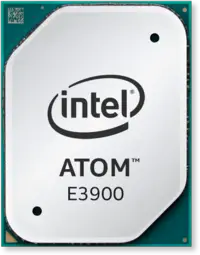
The Atom x5-E3930 is a 64-bit dual-core x86 system on a chip set introduced by Intel in early 2017. This ultra-low power MPU, which was specifically designed for the IoTs, operates at 1.3 GHz and has a TDP of 6.5 W. This chip is based on the Goldmont, manufactured on Intel's enhanced 14 nm process.
Cache[edit]
- Main article: Goldmont § Cache
| Cache Info [Edit Values] | ||
| L1I$ | 64 KiB 65,536 B 0.0625 MiB |
2x32 KiB 8-way set associative (per core) |
| L1D$ | 48 KiB 49,152 B 0.0469 MiB |
2x24 KiB 6-way set associative (per core) |
| L2$ | 2 MiB 2,048 KiB 2,097,152 B 0.00195 GiB |
2x1 MiB 16-way set associative (per 2 cores) |
| L3$ | 0 KiB 0 MiB 0 B 0 GiB |
No L3$ |
Memory controller[edit]
| Integrated Memory Controller | |
| Type | DDR3L-1866, LPDDR4-2133 |
| Controllers | 1 |
| Channels | 4 |
| ECC Support | Yes |
| Max bandwidth | 31.79 GiB/s |
| Bandwidth (single) | 15.89 GiB/s |
| Bandwidth (dual) | 31.79 GiB/s |
| Max memory | 8 GiB |
| Physical Address Extensions | 40 bit |
Graphics[edit]
| Integrated Graphic Information | |
| GPU | HD Graphics 500 |
| Device ID | 0x5A85 |
| Execution Units | 12 |
| Displays | 3 |
| Frequency | 400 MHz 0.4 GHz
400,000 KHz |
| Max frequency | 550 MHz 0.55 GHz
550,000 KHz |
| Max memory | 2 GiB 2,048 MiB
2,097,152 KiB 2,147,483,648 B |
| Output | DisplayPort, Embedded DisplayPort, HDMI, DSI |
| DirectX | 12 |
| OpenGL | 4.3 |
| OpenCL | 1.2 |
| OpenGL ES | 3.0 |
| HDMI | 1.4b |
| DP | 1.2 |
| eDP | 1.3 |
| Max HDMI Res | 3840x2160 @30 Hz |
| Max DSI Res | 2560x1600 @60 Hz |
| Max DP Res | 4096x2160 @60 Hz |
| Max eDP Res | 3840x2160 @60 Hz |
| Intel Quick Sync Video | |
| Intel Clear Video | |
- Video decode hardware acceleration including support for HEVC (H.265), H.264, MVC, VP8, VP9, MPEG2, VC-1, WMV9, JPEG/MJPEG.
- Video encode hardware acceleration including support for HEVC (H.265), H.264, MVC, VP8, VP9, JPEG/MJPEG.
Expansions[edit]
|
Expansion Options
|
||||||||||||||||||||||
|
||||||||||||||||||||||
Features[edit]
[Edit/Modify Supported Features]
|
Supported x86 Extensions & Processor Features
|
||||||||||||||||||||
|
||||||||||||||||||||
Die Shot[edit]
Intel Goldmont-based Atom E3900 SoC series die shot:

Documents[edit]
Facts about "Atom x5-E3930 - Intel"
| Has subobject "Has subobject" is a predefined property representing a container construct and is provided by Semantic MediaWiki. | Atom x5-E3930 - Intel#io + |
| base frequency | 1,300 MHz (1.3 GHz, 1,300,000 kHz) + |
| core count | 2 + |
| core name | Apollo Lake + |
| designer | Intel + |
| device id | 0x5A85 + |
| family | Atom x5 + |
| first announced | October 26, 2016 + |
| first launched | 2017 + |
| full page name | intel/atom x5/x5-e3930 + |
| has extended page tables support | true + |
| has feature | integrated gpu +, Advanced Encryption Standard Instruction Set Extension +, Burst Performance Technology +, Enhanced SpeedStep Technology + and Extended Page Tables + |
| has intel burst performance technology | true + |
| has intel enhanced speedstep technology | true + |
| has locked clock multiplier | true + |
| has second level address translation support | true + |
| has x86 advanced encryption standard instruction set extension | true + |
| instance of | microprocessor + |
| integrated gpu | HD Graphics 500 + |
| integrated gpu base frequency | 400 MHz (0.4 GHz, 400,000 KHz) + |
| integrated gpu max frequency | 550 MHz (0.55 GHz, 550,000 KHz) + |
| integrated gpu max memory | 2,048 MiB (2,097,152 KiB, 2,147,483,648 B, 2 GiB) + |
| isa | x86-64 + |
| isa family | x86 + |
| l1d$ description | 6-way set associative + |
| l1d$ size | 48 KiB (49,152 B, 0.0469 MiB) + |
| l1i$ description | 8-way set associative + |
| l1i$ size | 64 KiB (65,536 B, 0.0625 MiB) + |
| l2$ description | 16-way set associative + |
| l2$ size | 2 MiB (2,048 KiB, 2,097,152 B, 0.00195 GiB) + |
| l3$ description | No L3$ + |
| l3$ size | 0 MiB (0 KiB, 0 B, 0 GiB) + |
| ldate | 2017 + |
| main image |  + + |
| manufacturer | Intel + |
| market segment | Embedded + |
| max cpu count | 1 + |
| max junction temperature | 383.15 K (110 °C, 230 °F, 689.67 °R) + |
| max memory | 8,192 MiB (8,388,608 KiB, 8,589,934,592 B, 8 GiB, 0.00781 TiB) + |
| max pcie lanes | 4 + |
| microarchitecture | Goldmont + |
| min junction temperature | 233.15 K (-40 °C, -40 °F, 419.67 °R) + |
| model number | x5-E3930 + |
| name | Intel Atom x5-E3930 + |
| platform | Apollo Lake + |
| process | 14 nm (0.014 μm, 1.4e-5 mm) + |
| series | E3900 + |
| smp max ways | 1 + |
| tdp | 6.5 W (6,500 mW, 0.00872 hp, 0.0065 kW) + |
| technology | CMOS + |
| thread count | 2 + |
| turbo frequency (1 core) | 1,800 MHz (1.8 GHz, 1,800,000 kHz) + |
| word size | 64 bit (8 octets, 16 nibbles) + |