| Line 7: | Line 7: | ||
|introduction=2021 | |introduction=2021 | ||
|process=intel 7 (10nm ESF) | |process=intel 7 (10nm ESF) | ||
| − | |cores=8+8 | + | |cores=8 + 8 |
| − | |cores 2=6+8 | + | |cores 2=6 + 8 |
| − | |cores 3=6+0 | + | |cores 3=6 + 0 |
| + | |cores 4=2 + 8 | ||
|isa=x86-64 | |isa=x86-64 | ||
|l1i=32 KB | |l1i=32 KB | ||
Revision as of 03:21, 17 November 2021
| Edit Values | |
| Alder Lake µarch | |
| General Info | |
| Arch Type | CPU |
| Designer | Intel |
| Manufacturer | Intel |
| Introduction | 2021 |
| Process | intel 7 (10nm ESF) |
| Core Configs | "+8" can not be assigned to a declared number type with value 8. 8 + 8, "+8" can not be assigned to a declared number type with value 6. 6 + 8, "+0" can not be assigned to a declared number type with value 6. 6 + 0, "+8" can not be assigned to a declared number type with value 2. 2 + 8 |
| Instructions | |
| ISA | x86-64 |
| Cache | |
| L1I Cache | 32 KB/core |
| L1D Cache | 48 KB (P) / 64 KB (E)/core |
| L1 Cache | 80 KB (P) / 96 KB (E)/core |
| L2 Cache | 1.25 MB (P) / 2MB (4E)/core |
| L3 Cache | up to 30 MB |
| Cores | |
| Core Names | Golden Cove, Gracemont |
| Succession | |
Alder Lake (ADL) is Intel's successor to both Tiger Lake and Rocket Lake, an Intel 7-process based microarchitecture for mainstream workstations, desktops, and mobile devices. Alder Lake is Intel's first 10-nanometer-class proper successor to all prior generation of processors - spanning from ultra-low power to desktop and workstations. The microarchitecture was developed by Intel's R&D center in Haifa, Israel.
For desktop and mobile, Alder Lake is branded as 12th Generation Intel Core i3, Core i5, Core i7, and Core i9 processors.
Contents
[hide]Codenames
| Core | Abbrev | Platform | Target |
|---|---|---|---|
| Alder Lake M | ADL-M | Light notebooks, 2-in-1s detachable, tablets, conference room, computer sticks, etc. | |
| Alder Lake P | ADL-P | Ultimate mobile performance, mobile workstations, portable All-in-Ones (AiOs), Minis | |
| Alder Lake S | ADL-S | Desktop performance to value, AiOs, and minis |
Brands
Intel released Alder Lake under 3 main brand families for mainstream workstations, desktops, and mobile.
| Logo | Family | General Description | Differentiating Features | ||||||
|---|---|---|---|---|---|---|---|---|---|
| Cores | HT | AVX | AVX2 | TBT | TBMT | ||||
 |
Core i5 | Mid-range Performance | 10 (6+4) | ✔ | ✔ | ✔ | ✔ | ✘ | |
 |
Core i7 | High-end Performance | 12 (8+4) | ✔ | ✔ | ✔ | ✔ | ✔ | |
 |
Core i9 | Extreme Performance | 16 (8+8) | ✔ | ✔ | ✔ | ✔ | ✔ | |
Process Technology
Intel is planning Alder Lake to be built on an improved Intel 7 node (previously 10nm Enhanced SuperFin (ESF)). This will be the case for both the powerful Golden Cove cores, and Gracemont cores.
Compiler support
| Compiler | Arch-Specific | Arch-Favorable |
|---|---|---|
| ICC | -march=alderlake |
-mtune=alderlake
|
| GCC | -march=alderlake |
-mtune=alderlake
|
| LLVM | -march=alderlake |
-mtune=alderlake
|
| Visual Studio | /arch:AVX2 |
/tune:alderlake
|
CPUID
| Core | Extended Family |
Family | Extended Model |
Model |
|---|---|---|---|---|
| P | 0 | 0x6 | 0x9 | 0x7 |
| Family 6 Model 151 | ||||
| S | 0 | 0x6 | 0x9 | 0xA |
| Family 6 Model 154 | ||||
History
In January 2021 Intel teased Alder Lake in their CES 2021 speech. On the July 26th's Intel Accelerated webcast, CEO Pat Gelsinger hinted at the Alder Lake lineup being released at a future event called "Intel Innovation" which aired between October 27-28th.
Architecture
Key changes from Tiger Lake
- Core
- Hybrid Golden Cove (big core) & Gracemont (small core) microarchitecture
- At least 20% IPC improvements
- Intel 7 node
- Memory
- Support for DDR5
- Speeds of at least 4800MHz, up to 5600MHz
- Improved power delivery system
Overview
Alder Lake departs from all prior Intel SoCs by featuring the company's first mainstream implementation of a single-ISA heterogeneous multi-core microarchitecture. While not the first (Lakefield was), Alder Lake is the first to target all market segments from mobile to desktop and workstation. The overall microarchitecture builds on its its predecessor, Tigerlake but expends on its by integrating two vastly different types of cores - up to eight big cores based on the Golden Cove microarchitecture and up to eight small cores based on the Gracemont microarchitecture. The big cores are designed to push single-thread performance while the small cores are designed to push multi-thread power efficiency. By finely orchestrating thread scheduling based on performance demand, Alder Lake is able to provide both higher multi-threading performance-efficiency and better single-thread performance.
SoC design
| This section is empty; you can help add the missing info by editing this page. |
Die
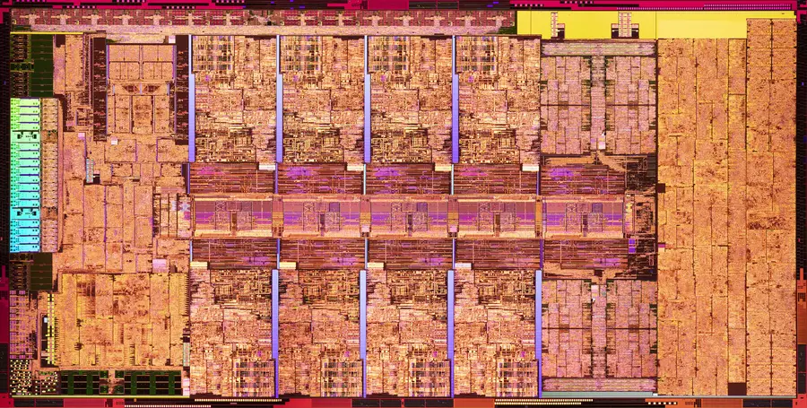
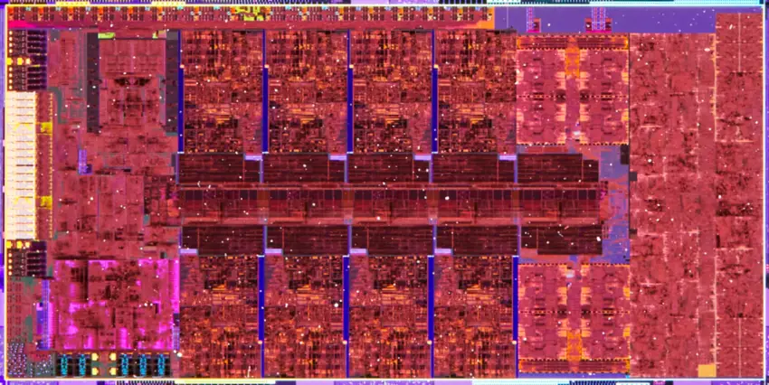
Alder Lake comes in four die variants depending on the market segment.
| Die | |||
|---|---|---|---|
| Name | Configuration | Dimensions | Area |
| ADL-S | 8P + 8E | 10.5 mm x 20.5 mm | 215.25 mm² |
| 6P + 8E | 10.5 mm x 15.5 mm | 162.75 mm² | |
| ADL-P | 6P + 8E | ||
| ADL-M | 2P + 8E | ||
ADL-S (8P+8E)
- 8 performance cores + 8 efficiency cores
- Intel 7 process
- 10.5 mm x 20.5 mm
- 215.25 mm² die size
ADL-S (6P+0E)
- 6 performance cores, no efficiency cores
- Intel 7 process
- 10.5 mm x 15.5 mm
- 162.75 mm² die size
Additional Shots
| codename | Alder Lake + |
| designer | Intel + |
| first launched | 2021 + |
| full page name | intel/microarchitectures/alder lake + |
| instance of | microarchitecture + |
| instruction set architecture | x86-64 + |
| manufacturer | Intel + |
| microarchitecture type | CPU + |
| name | Alder Lake + |


