From WikiChip
Difference between revisions of "intel/microarchitectures/alder lake"
(→History) |
|||
| Line 42: | Line 42: | ||
** Speeds of at least 4800MHz, up to 5600MHz | ** Speeds of at least 4800MHz, up to 5600MHz | ||
* Improved power delivery system | * Improved power delivery system | ||
| + | |||
| + | == Die == | ||
| + | Alder Lake comes in four die variants depending on the market segment. | ||
| + | |||
| + | {| class="wikitable" | ||
| + | ! colspan="4" | Die | ||
| + | |- | ||
| + | ! Name !! Configuration !! Dimensions !! Area | ||
| + | |- | ||
| + | | ADL-S || 8P + 8E || 10.5 mm x 20.5 mm || 215.25 mm² | ||
| + | |- | ||
| + | | ADL-S || 6P + 8E || 10.5 mm x 15.5 mm || 162.75 mm² | ||
| + | |- | ||
| + | | ADL-S || 6P + 8E | ||
| + | |- | ||
| + | | ADL-S || 2P + 8E | ||
| + | |} | ||
| + | |||
| + | === ADL-S (8P+8E) === | ||
| + | * 8 performance cores + 8 efficiency cores | ||
| + | * [[Intel 7]] process | ||
| + | * 10.5 mm x 20.5 mm | ||
| + | ** 215.25 mm² | ||
| + | |||
| + | :[[File:alder lake die.png|850px]] | ||
| + | |||
| + | === ADL-S (6P+0E) === | ||
| + | * 6 performance cores + 8 efficiency cores | ||
| + | * [[Intel 7]] process | ||
| + | * 10.5 mm x 15.5 mm | ||
| + | ** 162.75 mm² | ||
| + | |||
| + | === Additional Shots === | ||
| + | [[File:alder lake partial wafer shot.jpg|850px]] | ||
Revision as of 08:44, 3 November 2021
| Edit Values | |
| Alder Lake µarch | |
| General Info | |
| Arch Type | CPU |
| Designer | Intel |
| Manufacturer | Intel |
| Introduction | 2021 |
| Process | 10 nm |
| Core Configs | "+8" can not be assigned to a declared number type with value 8. 8+8, "+8" can not be assigned to a declared number type with value 6. 6+8, "+0" can not be assigned to a declared number type with value 6. 6+0 |
| Instructions | |
| ISA | x86-64 |
| Cores | |
| Core Names | Golden Cove, Gracemont |
| Succession | |
Alder Lake (ADL) is Intel's successor to Tiger Lake, a 10 nm microarchitecture for mainstream workstations, desktops, and mobile devices.
Contents
[hide]Process Technology
Intel is planning Alder Lake to be built on an improved Intel 7 node (previously 10nm Enhanced SuperFin (ESF)). This will be the case for both the powerful Golden Cove cores, and Gracemont cores.
History
In January 2021 Intel teased Alder Lake in their CES 2021 speech. On the July 26th's Intel Accelerated webcast, CEO Pat Gelsinger hinted at the Alder Lake lineup being released at a future event called "Intel Innovation" which aired between October 27-28th.
Architecture
Key changes from Tiger Lake
- Core
- Hybrid Golden Cove (big core) & Gracemont (small core) microarchitecture
- At least 20% IPC improvements
- Intel 7 node
- Memory
- Support for DDR5
- Speeds of at least 4800MHz, up to 5600MHz
- Improved power delivery system
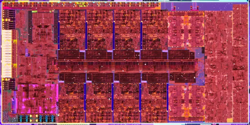
Die
Alder Lake comes in four die variants depending on the market segment.
| Die | |||
|---|---|---|---|
| Name | Configuration | Dimensions | Area |
| ADL-S | 8P + 8E | 10.5 mm x 20.5 mm | 215.25 mm² |
| ADL-S | 6P + 8E | 10.5 mm x 15.5 mm | 162.75 mm² |
| ADL-S | 6P + 8E | ||
| ADL-S | 2P + 8E | ||
ADL-S (8P+8E)
- 8 performance cores + 8 efficiency cores
- Intel 7 process
- 10.5 mm x 20.5 mm
- 215.25 mm²
ADL-S (6P+0E)
- 6 performance cores + 8 efficiency cores
- Intel 7 process
- 10.5 mm x 15.5 mm
- 162.75 mm²
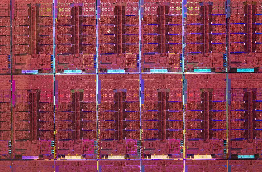
Additional Shots
Facts about "Alder Lake - Microarchitectures - Intel"
| codename | Alder Lake + |
| designer | Intel + |
| first launched | 2021 + |
| full page name | intel/microarchitectures/alder lake + |
| instance of | microarchitecture + |
| instruction set architecture | x86-64 + |
| manufacturer | Intel + |
| microarchitecture type | CPU + |
| name | Alder Lake + |
| process | 10 nm (0.01 μm, 1.0e-5 mm) + |

