(mars i) |
|||
| (7 intermediate revisions by the same user not shown) | |||
| Line 42: | Line 42: | ||
{{main|phytium/microarchitectures/xiaomi|l1=Xiaomi Core}} | {{main|phytium/microarchitectures/xiaomi|l1=Xiaomi Core}} | ||
See {{\\|Xiaomi|Xiaomi Core}}. | See {{\\|Xiaomi|Xiaomi Core}}. | ||
| + | |||
| + | == SoC == | ||
| + | |||
| + | === Panel Architecture === | ||
| + | [[File:xiaomi panel-based data affinity architecture.png|right|450px]] | ||
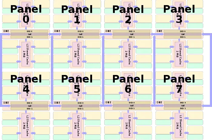
| + | Phytium organizes their processors using a grid-layout they call '''Panels''' they call '''Panel-based data affinity architecture'''. Each panel consists of 8 independent [[ARMv8]]-compatible cores. Phytium "Mars" processor consists of 8 such panels for a total of [[64 cores]]. Panels are interconnected with a 2-dimensional mesh network-on-a-chip [[level 2 cache]] with 4 MiB per panel for a total of 32 MiB. | ||
| + | |||
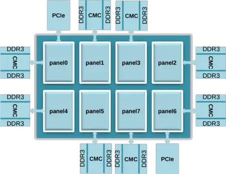
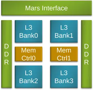
| + | In addition to the main die, Mars uses an additional '''Cache & Memory chips''' ('''CMC''') auxiliary chips. "Mars" uses 8 such chips connected to the main die providing 16 MiB of [[level 3 cache]] for a total of 128 MiB as well as 8 dual-channel DDR3-1600 [[memory controller]]s for a total maximum bandwidth of 204 GiB/s. Mars also provides two 16-lane PCIe 3.0 interfaces. The chips incorporates ECC and parity protection on all caches, tags, and TLBs. | ||
| + | |||
| + | ==== Panel ==== | ||
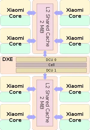
| + | Each Panel consists of 8 cores - each [[ARMv8]]-compatible, supporting AArch32 and AArch64 modes, Exception Levels EL0-EL3, as well as ASIMD-128 operations. Each core has its own inclusive [[L1 cache]] and a shared [[L2 cache]] (4 MiB per panel). Each panel contains two '''Directory Control Units''' ('''DCU''') which are in charge of maintaining directory-based [[cache coherency]] and one routing cell for managing the inter-panel communication. | ||
| + | |||
| + | On TSMC's [[28 nm process]], a panel is 6,000 µm x 10,600 µm (63.6 mm²). | ||
| + | |||
| + | {| style="border-spacing: 15px;" | ||
| + | | [[File:xiaomi panel.png|400px]] || || [[File:xiaomi panel die (28nm).png|300px]] | ||
| + | |} | ||
| + | |||
| + | ==== Cache & Memory Chip (CMC) ==== | ||
| + | [[File:xiaomi cmc.png|right|300px]] | ||
| + | The solve the complexity involved in having more than eight memory controllers on a chip, Xiaomi uses a coupled auxiliary '''Cache & Memory Chip''' ('''CMC''') to scale the bandwidth with computing power. In the case of Phytium "Mars" chip which contains 64 cores on 8 panels, eight CMC chips are used which provides 16 DDR3 controllers (8x2) along with 16 MiB of data L3 cache and 2 MiB of data ECC. Phytium proprietary interface is used between the processor and the CMC chip. | ||
| + | |||
| + | {| | ||
| + | | [[File:xiaomi latency.png|600px]] || | ||
| + | {| class="wikitable" | ||
| + | ! Memory access !! Latency(ns) | ||
| + | |- | ||
| + | |Local L1 cache hit || ~2 | ||
| + | |- | ||
| + | |Local L2 cache hit || ~8 | ||
| + | |- | ||
| + | |Affinitive L2 cache hit || ~20 | ||
| + | |- | ||
| + | |Affinitive L3 cache hit || ~36 | ||
| + | |- | ||
| + | |Affinitive DDR access || ~70 | ||
| + | |} | ||
| + | |} | ||
| + | * Panel & NoC operates @ 2 GHz | ||
| + | * CMC operates @ 1.5 GHz | ||
| + | |||
| + | === Interconnects & Hawk === | ||
| + | '''Hawk''' is Pythium cache coherence protocol which implements a distributed directory-based global cache coherency across all the panels. Hawk is a [[MOESI]]-like package-based protocol. The network has a node on each panel called a '''Directory Control Unit''' ('''DCU''') which is responsible for interfacing between the L2 caches in each panel to the CMCs (see [[#Panel_Architecture|§ Panel Architecture]]). Phytium noted that it's optimized for exclusive atomic accesses. | ||
| + | |||
| + | Xiaomi implements a 2D concentrated mesh architecture on-die connecting each of the panels. Phytium "Mars" chip contains 8 panels which are organized in two rows of four panels each. Switching is relatively low latency with 3 cycles per hop. On average, packets will have around 9 cycles latency from any other panel. This network results in a bandwidth of 384 GiB/s each cell. | ||
| + | |||
| + | {| | ||
| + | | [[File:xiaomi 2d network.png|600px]] || | ||
| + | {| class="wikitable" style="text-align: center;" | ||
| + | ! Destination !! Latency | ||
| + | |- | ||
| + | | 0 || 3 | ||
| + | |- | ||
| + | | 1 || 6 | ||
| + | |- | ||
| + | | 2 || 9 | ||
| + | |- | ||
| + | | 3 || 12 | ||
| + | |- | ||
| + | | 4 || 15 | ||
| + | |- | ||
| + | | 5 || 12 | ||
| + | |- | ||
| + | | 6 || 9 | ||
| + | |- | ||
| + | | 7 || 6 | ||
| + | |- | ||
| + | | Average || 9 | ||
| + | |} | ||
| + | |} | ||
== Die == | == Die == | ||
| Line 47: | Line 117: | ||
* Mars is fabricated on [[TSMC]]'s [[28 nm process]] | * Mars is fabricated on [[TSMC]]'s [[28 nm process]] | ||
* 10 metal layers | * 10 metal layers | ||
| − | * ~180 million instances | + | * 4,800,000,000 transistors |
| + | ** ~180 million instances | ||
* 639.576 mm² die size | * 639.576 mm² die size | ||
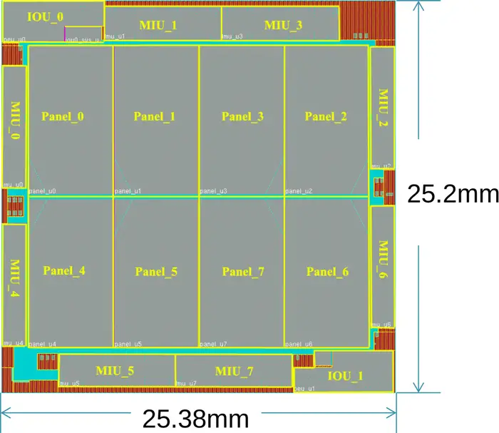
| + | ** 25.38 mm x 25.2 mm | ||
* FCBGA Package | * FCBGA Package | ||
** ~3000 pins | ** ~3000 pins | ||
| Line 55: | Line 127: | ||
:[[File:xiaomi floor plan.png|class=wikichip_ogimage|700px]] | :[[File:xiaomi floor plan.png|class=wikichip_ogimage|700px]] | ||
| + | |||
| + | == All Mars I Processors == | ||
| + | <!-- NOTE: | ||
| + | This table is generated automatically from the data in the actual articles. | ||
| + | If a microprocessor is missing from the list, an appropriate article for it needs to be | ||
| + | created and tagged accordingly. | ||
| + | |||
| + | Missing a chip? please dump its name here: https://en.wikichip.org/wiki/WikiChip:wanted_chips | ||
| + | --> | ||
| + | {{comp table start}} | ||
| + | <table class="comptable sortable tc4"> | ||
| + | {{comp table header|main|6:List of Mars I-based Processors}} | ||
| + | {{comp table header|cols|Launched|Cores|L2|%Frequency|%TDP}} | ||
| + | {{#ask: [[Category:microprocessor models by phytium]] [[microarchitecture::Mars I]] | ||
| + | |?full page name | ||
| + | |?model number | ||
| + | |?first launched | ||
| + | |?core count | ||
| + | |?l2$ size | ||
| + | |?base frequency#GHz | ||
| + | |?tdp#W | ||
| + | |format=template | ||
| + | |template=proc table 3 | ||
| + | |userparam=7 | ||
| + | |mainlabel=- | ||
| + | }} | ||
| + | {{comp table count|ask=[[Category:microprocessor models by phytium]] [[microarchitecture::Mars I]]}} | ||
| + | </table> | ||
| + | {{comp table end}} | ||
| + | |||
| + | == Bibliography == | ||
| + | * {{bib|hc|27|Phytium}} | ||
Latest revision as of 16:49, 15 October 2019
| Edit Values | |
| Mars I µarch | |
| General Info | |
| Arch Type | CPU |
| Designer | Phytium |
| Manufacturer | TSMC |
| Introduction | 2017 |
| Process | 28 nm |
| Core Configs | 64 |
| Pipeline | |
| Type | Superscalar, Pipelined |
| OoOE | Yes |
| Speculative | Yes |
| Reg Renaming | Yes |
| Instructions | |
| ISA | ARMv8 |
| Succession | |
Mars I is the first many-core ARM SoC microarchitecture designed by Phytium Technology for the Chinese server market.
Contents
Process technology[edit]
Mars I is designed for TSMC's 28 nm process.
Architecture[edit]
- 64 ARM cores
- 28 nm process
- 2 GHz
- FTC-661/0 Xiaomi core
- System memory
- DDR3
- 1600 MT/s
This list is incomplete; you can help by expanding it.
Block diagram[edit]
Entire SoC[edit]
Panel[edit]
Core[edit]
- Main article: Xiaomi Core
See Xiaomi Core.
SoC[edit]
Panel Architecture[edit]
Phytium organizes their processors using a grid-layout they call Panels they call Panel-based data affinity architecture. Each panel consists of 8 independent ARMv8-compatible cores. Phytium "Mars" processor consists of 8 such panels for a total of 64 cores. Panels are interconnected with a 2-dimensional mesh network-on-a-chip level 2 cache with 4 MiB per panel for a total of 32 MiB.
In addition to the main die, Mars uses an additional Cache & Memory chips (CMC) auxiliary chips. "Mars" uses 8 such chips connected to the main die providing 16 MiB of level 3 cache for a total of 128 MiB as well as 8 dual-channel DDR3-1600 memory controllers for a total maximum bandwidth of 204 GiB/s. Mars also provides two 16-lane PCIe 3.0 interfaces. The chips incorporates ECC and parity protection on all caches, tags, and TLBs.
Panel[edit]
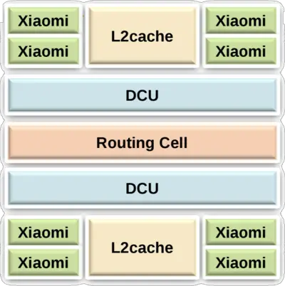
Each Panel consists of 8 cores - each ARMv8-compatible, supporting AArch32 and AArch64 modes, Exception Levels EL0-EL3, as well as ASIMD-128 operations. Each core has its own inclusive L1 cache and a shared L2 cache (4 MiB per panel). Each panel contains two Directory Control Units (DCU) which are in charge of maintaining directory-based cache coherency and one routing cell for managing the inter-panel communication.
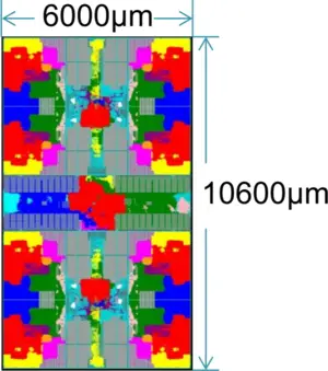
On TSMC's 28 nm process, a panel is 6,000 µm x 10,600 µm (63.6 mm²).
 |
|
Cache & Memory Chip (CMC)[edit]
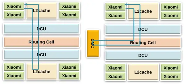
The solve the complexity involved in having more than eight memory controllers on a chip, Xiaomi uses a coupled auxiliary Cache & Memory Chip (CMC) to scale the bandwidth with computing power. In the case of Phytium "Mars" chip which contains 64 cores on 8 panels, eight CMC chips are used which provides 16 DDR3 controllers (8x2) along with 16 MiB of data L3 cache and 2 MiB of data ECC. Phytium proprietary interface is used between the processor and the CMC chip.
 |
|
- Panel & NoC operates @ 2 GHz
- CMC operates @ 1.5 GHz
Interconnects & Hawk[edit]
Hawk is Pythium cache coherence protocol which implements a distributed directory-based global cache coherency across all the panels. Hawk is a MOESI-like package-based protocol. The network has a node on each panel called a Directory Control Unit (DCU) which is responsible for interfacing between the L2 caches in each panel to the CMCs (see § Panel Architecture). Phytium noted that it's optimized for exclusive atomic accesses.
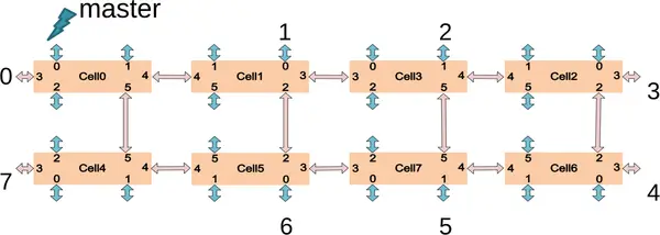
Xiaomi implements a 2D concentrated mesh architecture on-die connecting each of the panels. Phytium "Mars" chip contains 8 panels which are organized in two rows of four panels each. Switching is relatively low latency with 3 cycles per hop. On average, packets will have around 9 cycles latency from any other panel. This network results in a bandwidth of 384 GiB/s each cell.
 |
|
Die[edit]
SoC[edit]
- Mars is fabricated on TSMC's 28 nm process
- 10 metal layers
- 4,800,000,000 transistors
- ~180 million instances
- 639.576 mm² die size
- 25.38 mm x 25.2 mm
- FCBGA Package
- ~3000 pins
- 0.9 VCORE, 1.8 VIO
- 2 GHz, 120 W
All Mars I Processors[edit]
| List of Mars I-based Processors | ||||||
|---|---|---|---|---|---|---|
| Model | Launched | Cores | L2 | Frequency | TDP | |
| FT-2000/64 | 2017 | 64 | 32 MiB 32,768 KiB 33,554,432 B 0.0313 GiB | 2 GHz 2,000 MHz 2,000,000 kHz | 120 W 120,000 mW 0.161 hp 0.12 kW | |
| Count: 1 | ||||||
Bibliography[edit]
- Phytium, IEEE Hot Chips 27 Symposium (HCS) 2015.
| codename | Mars I + |
| core count | 64 + |
| designer | Phytium + |
| first launched | 2017 + |
| full page name | phytium/microarchitectures/mars i + |
| instance of | microarchitecture + |
| instruction set architecture | ARMv8 + |
| manufacturer | TSMC + |
| microarchitecture type | CPU + |
| name | Mars I + |
| process | 28 nm (0.028 μm, 2.8e-5 mm) + |
