(→Execution Units) |
|||
| Line 90: | Line 90: | ||
===== Execution Units ===== | ===== Execution Units ===== | ||
| − | {{ | + | The A76 issue is 8-wide, allow for up to eight µOPs to execute each cycle. The execution units can be grouped into three categories: integer, advanced SIMD, and memory. |
| + | |||
| + | There are four pipelines in the integer cluster - three for general math operations and a dedicate branch ALU. All three ports have a simple ALU. The third port has support for complex arithmetic (e.g. MAC, DIV). | ||
| + | |||
| + | There are two ASIMD/FP execution pipelines. In the {{\\|Cortex-A75}}, each of the pipelines were 64-bit wide, on the A76, they were doubled to 128-bit. This means each pipeline is capable of 2 double-precision operations, 4 single-precision, 8 half-precision, or 16 8-bit integer operations. | ||
===== Memory subsystem ===== | ===== Memory subsystem ===== | ||
Revision as of 03:24, 28 December 2018
| Edit Values | |
| Cortex-A76 µarch | |
| General Info | |
| Arch Type | CPU |
| Designer | ARM Holdings |
| Manufacturer | TSMC |
| Introduction | May 31, 2018 |
| Process | 7 nm |
| Core Configs | 1, 2, 4 |
| Pipeline | |
| OoOE | Yes |
| Speculative | Yes |
| Reg Renaming | Yes |
| Stages | 13 |
| Decode | 4-way |
| Instructions | |
| ISA | ARMv8.2 |
| Extensions | FPU, NEON |
| Cache | |
| L1I Cache | 64 KiB/core 4-way set associative |
| L1D Cache | 64 KiB/core 4-way set associative |
| L2 Cache | 256-512 KiB/core 8-way set associative |
| L3 Cache | 0-4 MiB/Cluster |
| Succession | |
| Contemporary | |
| Ares | |
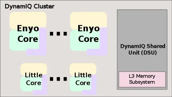
Cortex-A76 (codename Enyo) is the successor to the Cortex-A75, a low-power high-performance ARM microarchitecture designed by ARM Holdings for the mobile market. This microarchitecture is designed as a synthesizable IP core and is sold to other semiconductor companies to be implemented in their own chips. The Cortex-A76, which implemented the ARMv8.2 ISA, is the a performant core which is often combined with a number of lower power cores (e.g. Cortex-A55) in a DynamIQ big.LITTLE configuration to achieve better energy/performance.
History
Development of the Cortex-A76 started in 2013. Arm formally announced Enyo during Arm Tech Day on May 31 2018.
Process Technology
Though the Cortex-A76 may be fabricated on various different process nodes, it has been primarily designed for the 12 nm, 7 nm, and 5 nm process nodes.
Architecture
Key changes from Cortex-A75
Block Diagram
Typical SoC
Individual Core
Memory Hierarchy
The Cortex-A76 has a private L1I, L1D, and L2 cache.
- Cache
- L1I Cache
- 64 KiB, 4-way set associative
- 64-byte cache lines
- optional parity
- L1D Cache
- L1I Cache
The A76 TLB consists of dedicated L1 TLB for instruction cache (ITLB) and another one for data cache (DTLB). Additionally, there is a unified L2 TLB (STLB).
- TLBs
- ITLB
- 4 KiB, 16 KiB, 64 KiB, 2 MiB, and 32 MiB page sizes
- 48-entry fully associative
- ITLB
Overview
The Cortex-A76 is a high-performance synthesizable core designed by Arm as the successor to the Cortex-A75. It is delivered as Register Transfer Level (RTL) description in Verilog and is designed. This core supports the ARMv8.2 extension as well as a number of other partial extensions. The A76 is a 4-way superscalar out-of-order processor with a private level 1 and level 2 caches. It is designed to be implemented inside the DynamIQ Shared Unit (DSU) cluster along with other cores (e.g., with little cores such as the Cortex-A55)
Core
The Cortex-A76 succeeds the Cortex-A75. It is designed to take advantage of the 7 nm node in order to deliver up to 35% higher performance and up to 40% lower power (compared to the A75 on the 10 nm node). It's worth noting that the A76 brings higher performance at a slight hit to the area by going wider. On the 7 nm process, the Cortex-A76 targets frequencies of 3 GHz and higher.
Pipeline
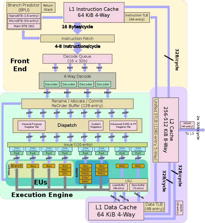
The Cortex-A76 is a complex, 4-way superscalar out-of-order processor with an 8-issue back end. It has a 64 KiB level 1 instruction cache and a 64 KiB level 1 data cachealong with a private level 2 cache that is configurable as either 256 KiB (1 bank) or 512 KiB (2 banks)
Front-end
Each cycle, up to 16 bytes are fetched from the L1 instruction cache. The instruction fetch works in tandem with the branch predictor in order to ensure the instruction stream is ready to be fetched. The Cortex-A76 has a fixed 64 KiB L1I cache. It is 4-way set associative and supports optional parity protection.
From the instruction fetch, up to four 32-bit instructions are sent to the decode queue (DQ) each cycle. For narrower 16-bit instructions (i.e., Thumb), this means up to eight instructions get queued. The A76 features a 4-way decode. Up to four instructions may be decoded into macro-operations each cycle.
Back-end
The Cortex-A76 back-end handles the execution of out-of-order operations. The design is largely inherited from the Cortex-A75 but has been adjusted for higher throughput.
Renaming & Allocation
From the front-end, up to four macro-operations may be sent each cycle to be renamed. The ROB has a capacity of up to 128 instructions in flight. Micro-operations are broken down into their µOP constituents and are scheduled for execution. From here, µOPs are sent to the instruction issue which controls when they can be dispatched to the execution pipelines. µOPs are queued in eight independent issue queues (120 entries in total).
Execution Units
The A76 issue is 8-wide, allow for up to eight µOPs to execute each cycle. The execution units can be grouped into three categories: integer, advanced SIMD, and memory.
There are four pipelines in the integer cluster - three for general math operations and a dedicate branch ALU. All three ports have a simple ALU. The third port has support for complex arithmetic (e.g. MAC, DIV).
There are two ASIMD/FP execution pipelines. In the Cortex-A75, each of the pipelines were 64-bit wide, on the A76, they were doubled to 128-bit. This means each pipeline is capable of 2 double-precision operations, 4 single-precision, 8 half-precision, or 16 8-bit integer operations.
Memory subsystem
| This section is empty; you can help add the missing info by editing this page. |
Bibliography
- Arm Tech Day, 2018
| codename | Cortex-A76 + |
| core count | 1 +, 2 + and 4 + |
| designer | ARM Holdings + |
| first launched | May 31, 2018 + |
| full page name | arm holdings/microarchitectures/cortex-a76 + |
| instance of | microarchitecture + |
| instruction set architecture | ARMv8.2 + |
| manufacturer | TSMC + |
| microarchitecture type | CPU + |
| name | Cortex-A76 + |
| pipeline stages | 13 + |
| process | 7 nm (0.007 μm, 7.0e-6 mm) + |

