From WikiChip
Difference between revisions of "amd/microarchitectures/zen 2"
(→Architecture) |
(→Key changes from {{\\|Zen}}) |
||
| Line 53: | Line 53: | ||
=== Key changes from {{\\|Zen}} === | === Key changes from {{\\|Zen}} === | ||
* [[7 nm process]] (from [[14 nm]]) | * [[7 nm process]] (from [[14 nm]]) | ||
| − | * PCIe 4.0 (from 3.0) | + | * Core |
| + | ** Front-end | ||
| + | *** Improved [[branch prediction unit]] | ||
| + | **** Improved prefetcher | ||
| + | *** Improved µOP cache tags | ||
| + | *** Improved µOP cache | ||
| + | **** Larger µOP cache (?? enters, up from 2048) | ||
| + | *** Increased dispatch bandwidth | ||
| + | ** Back-end | ||
| + | *** Increased retire bandwidth (??-wide, up from 8-wide) | ||
| + | *** FPU | ||
| + | **** 2x wider datapath (256-bit, up from 128-bit) | ||
| + | **** 2x wider EUs (256-bit FMAs, up from 128-bit FMAs) | ||
| + | **** 2x wider LSU (2x256-bit L/S, up from 128-bit) | ||
| + | * I/O | ||
| + | ** PCIe 4.0 (from 3.0) | ||
| + | ** {{amd|Infinity Fabric}} 2 | ||
| + | *** 2.3x transfer rate per link (25 GT/s, up from ~10.6 GT/s) | ||
| + | |||
{{expand list}} | {{expand list}} | ||
Revision as of 22:09, 17 November 2018
| Edit Values | |
| Zen 2 µarch | |
| General Info | |
| Arch Type | CPU |
| Designer | AMD |
| Manufacturer | TSMC |
| Introduction | 2019 |
| Process | 7 nm |
| Succession | |
Zen 2 is a planned microarchitecture being developed by AMD as a successor to Zen+. Zen 2 is expected to be succeeded by Zen 3.
Contents
History
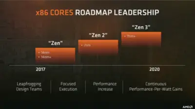
Zen 2 is set to succeed Zen in the future, sometimes around 2019. In February of 2017 Lisa Su, AMD's CEO announced their future roadmap to include Zen 2 and later Zen 3. On Investor's Day May 2017 Jim Anderson, AMD Senior Vice President, confirmed that Zen 2 is set to utilize 7 nm process.
Codenames
| Core | C/T | Target |
|---|---|---|
| Rome | Up to 64/128 | High-end server multiprocessors |
| Castle Peak | ?/? | workstation & enthusiasts market processors |
| Matisse | ?/? | Mainstream to high-end desktops & enthusiasts market processors |
| Picasso | ?/? | Mainstream desktop & mobile processors with GPU |
Process technology
Zen 2 is fabricated on TSMC's 7 nm process.
Compiler support
| Compiler | Arch-Specific | Arch-Favorable |
|---|---|---|
| GCC | -march=znver2 |
-mtune=znver2
|
- Note: Initial support in GCC 9.
Architecture
Key changes from Zen
- 7 nm process (from 14 nm)
- Core
- Front-end
- Improved branch prediction unit
- Improved prefetcher
- Improved µOP cache tags
- Improved µOP cache
- Larger µOP cache (?? enters, up from 2048)
- Increased dispatch bandwidth
- Improved branch prediction unit
- Back-end
- Increased retire bandwidth (??-wide, up from 8-wide)
- FPU
- 2x wider datapath (256-bit, up from 128-bit)
- 2x wider EUs (256-bit FMAs, up from 128-bit FMAs)
- 2x wider LSU (2x256-bit L/S, up from 128-bit)
- Front-end
- I/O
- PCIe 4.0 (from 3.0)
- Infinity Fabric 2
- 2.3x transfer rate per link (25 GT/s, up from ~10.6 GT/s)
This list is incomplete; you can help by expanding it.
New instructions
Zen 2 introduced a number of new x86 instructions:
-
CLWB- Force cache line write-back without flush -
RDPID- Read Processor ID -
WBNOINVD- Force cache line write-back without invalidation
Bibliography
- AMD 'Tech Day', February 22, 2017
- AMD 2017 Financial Analyst Day, May 16, 2017
- AMD GCC 9 znver2 enablement patch
- AMD 'Next Horizon', November 6, 2018
See Also
- Intel Ice Lake
Facts about "Zen 2 - Microarchitectures - AMD"
| codename | Zen 2 + |
| designer | AMD + |
| first launched | 2019 + |
| full page name | amd/microarchitectures/zen 2 + |
| instance of | microarchitecture + |
| manufacturer | TSMC + |
| microarchitecture type | CPU + |
| name | Zen 2 + |
| process | 7 nm (0.007 μm, 7.0e-6 mm) + |

