From WikiChip
Difference between revisions of "intel/chipsets/poulsbo"
| Line 11: | Line 11: | ||
| developer 2 = Imagination Technologies | | developer 2 = Imagination Technologies | ||
| manufacturer = Intel | | manufacturer = Intel | ||
| − | | first announced = | + | | first announced = April 18, 2007 |
| − | | first launched = | + | | first launched = March 2, 2008 |
| proc = 0.13 μm | | proc = 0.13 μm | ||
| tech = CMOS | | tech = CMOS | ||
Revision as of 21:40, 2 April 2017
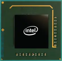
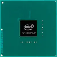
Poulsbo is a chipset for Intel's first generation of Atom processors based on the Bonnell microarchitecture.
Contents
Overview
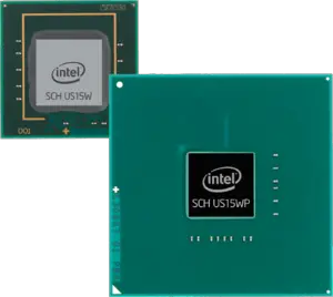
The Poulsbo chipset, part of the Menlow, offers the memory controller along with the much of the southbridge. Unlike all previous front-side bus signaling logic which used GTL, to allow for more power saving, Poulsbo became the first chipset to support CMOS signaling as well. Such functionality was only offered by the Silverthorne-based processors. In 2009 Intel released a second variant of Poulsbo in a larger package.
Features
- Intel GMA 500 GPU
- Licensed Imagination Technologies PowerVR SGX 535 graphics core + PowerVR VXD370 H.264/MPEG-4 AVC playback
| This section requires expansion; you can help adding the missing info. |
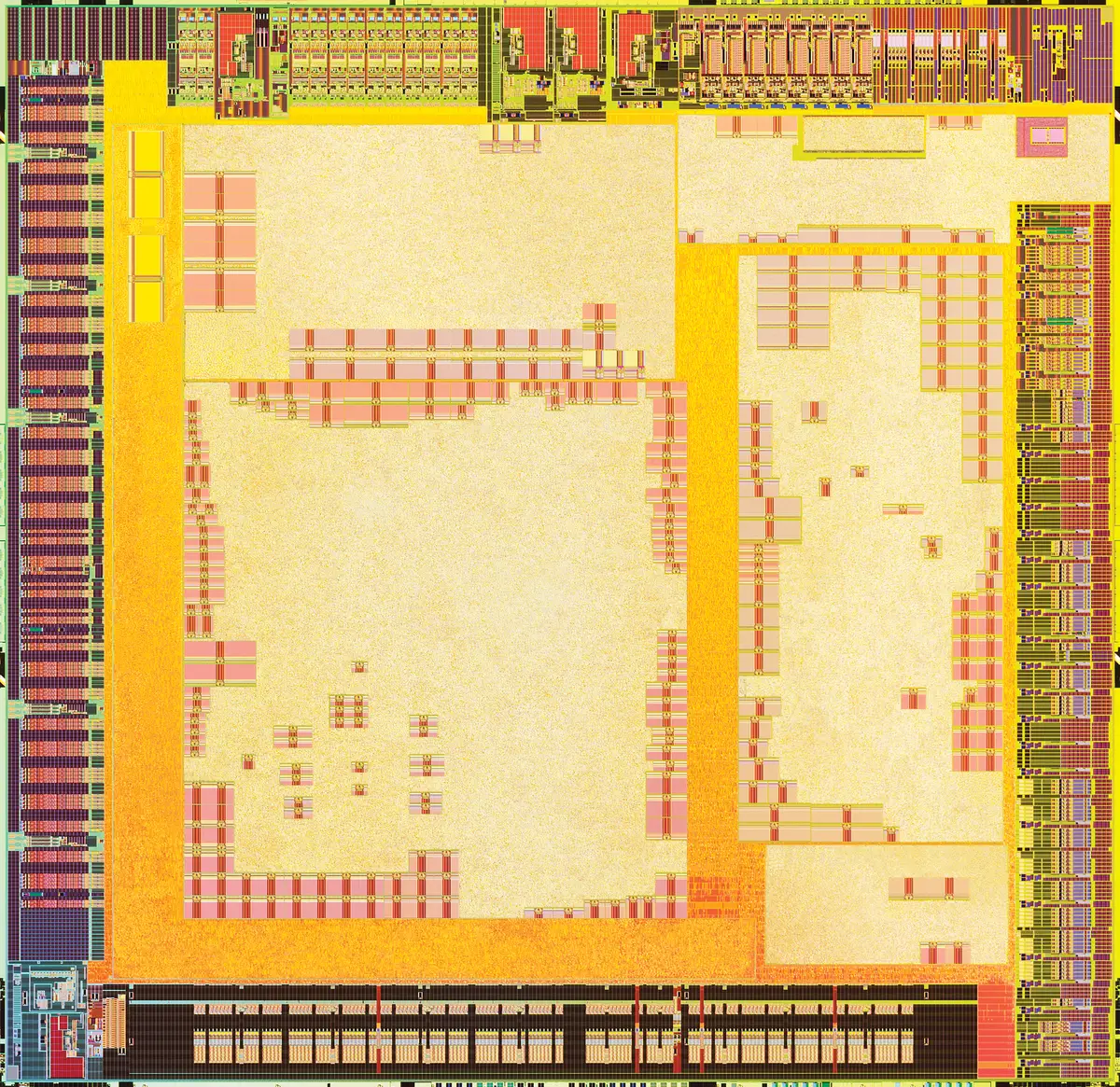
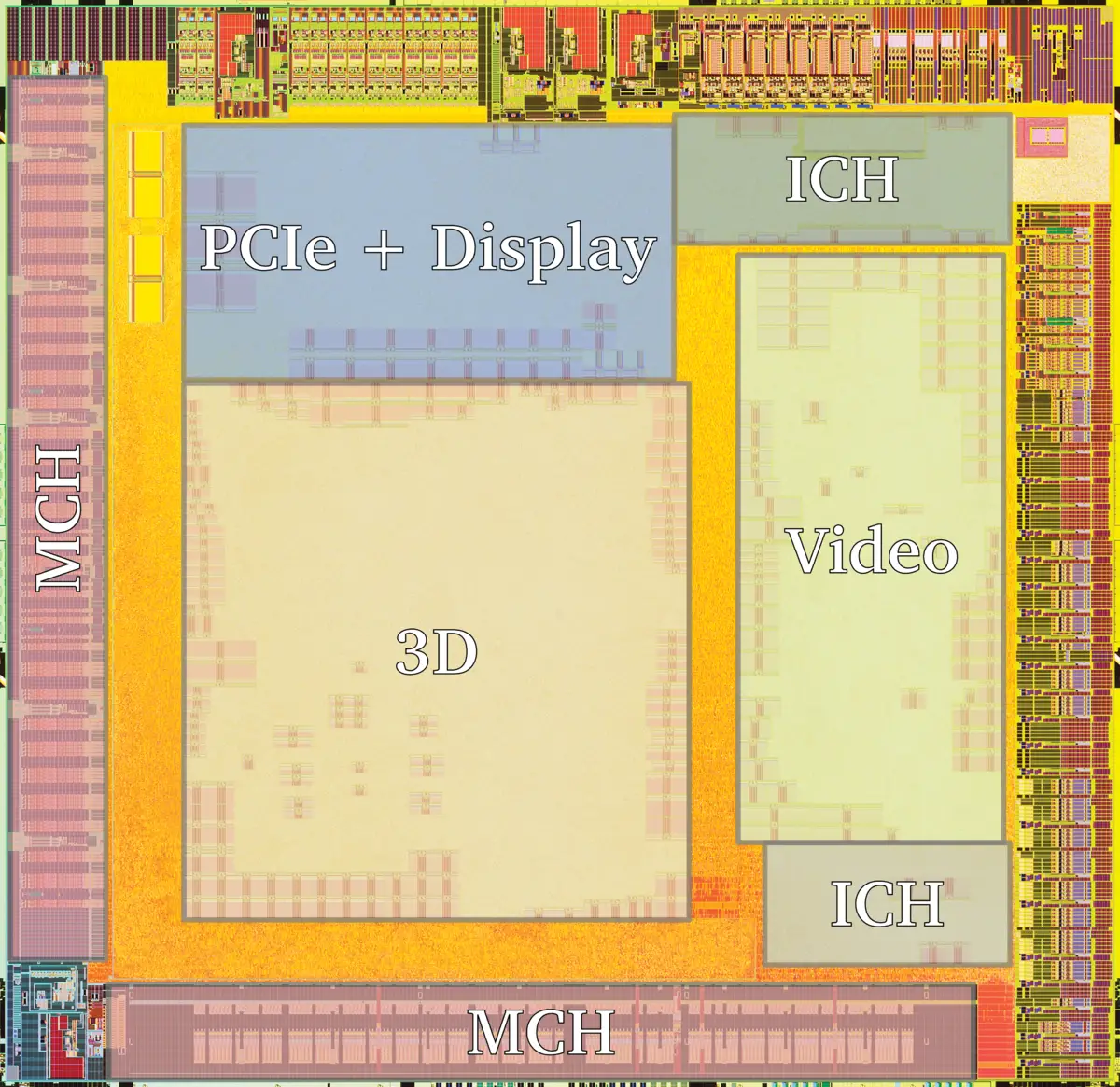
Die Shot
- 0.13 μm process
- 22 mm x 22 mm package
Documents
Facts about "Poulsbo - Chipsets - Intel"
| bus speed | 533 MHz (0.533 GHz, 533,000 kHz) + |
| bus type | FSB + |
| designer | Intel + and Imagination Technologies + |
| first announced | April 18, 2007 + |
| first launched | March 2, 2008 + |
| instance of | chipset + |
| manufacturer | Intel + |
| name | Poulsbo + |
| process | 130 nm (0.13 μm, 1.3e-4 mm) + |
| technology | CMOS + and GTL + |
