Semiconductor & Computer Engineering
From WikiChip
File list
This special page shows all uploaded files.
First page |
Previous page |
Next page |
Last page |
| Date | Name | Thumbnail | Size | User | Description | Versions |
|---|---|---|---|---|---|---|
| 15:28, 28 January 2017 | Compute Architecture of Intel Processor Graphics Gen8.pdf (file) |  |
2.31 MB | ChipIt | The Compute Architecture of {{intel|Gen8|Intel® Processor Graphics Gen8|l=arch}} Version 1.1 | 1 |
| 15:29, 28 January 2017 | 5th-gen-core-graphics-developer-guide.pdf (file) |  |
980 KB | ChipIt | Graphics API Developer’s Guide For 5th Generation Intel® Core Processors | 1 |
| 15:32, 28 January 2017 | Compute Architecture of Intel Processor Graphics Gen7dot5 Aug4 2014.pdf (file) |  |
1.99 MB | ChipIt | The Compute Architecture of {{intel|Gen7.5|Intel Processor Graphics Gen7.5|l=arch}} Version 1.0 | 1 |
| 15:32, 28 January 2017 | 4th-gen-core-graphics-dev-guide.pdf (file) |  |
1.15 MB | ChipIt | Developer's Guide for Intel® Processor Graphics For 4th Generation Intel® Core Processors | 1 |
| 15:39, 28 January 2017 | Ivy Bridge Graphics Developers Guide2.pdf (file) |  |
506 KB | ChipIt | DirectX* Developer’s Guide for Intel® Processor Graphics Maximizing Performance on the New Intel Microarchitecture Codenamed {{intel|Ivy Bridge|l=arch}} | 1 |
| 15:42, 28 January 2017 | Sandy Bridge Intel HD Graphics DirectX Developer s Guide 2dot9dot6.pdf (file) |  |
604 KB | ChipIt | Intel Processor Graphics DirectX* Developer's Guide How to maximize graphics performance on Intel {{intel|Sandy Bridge|microarchitecture codename Sandy Bridge|l=arch}}. | 1 |
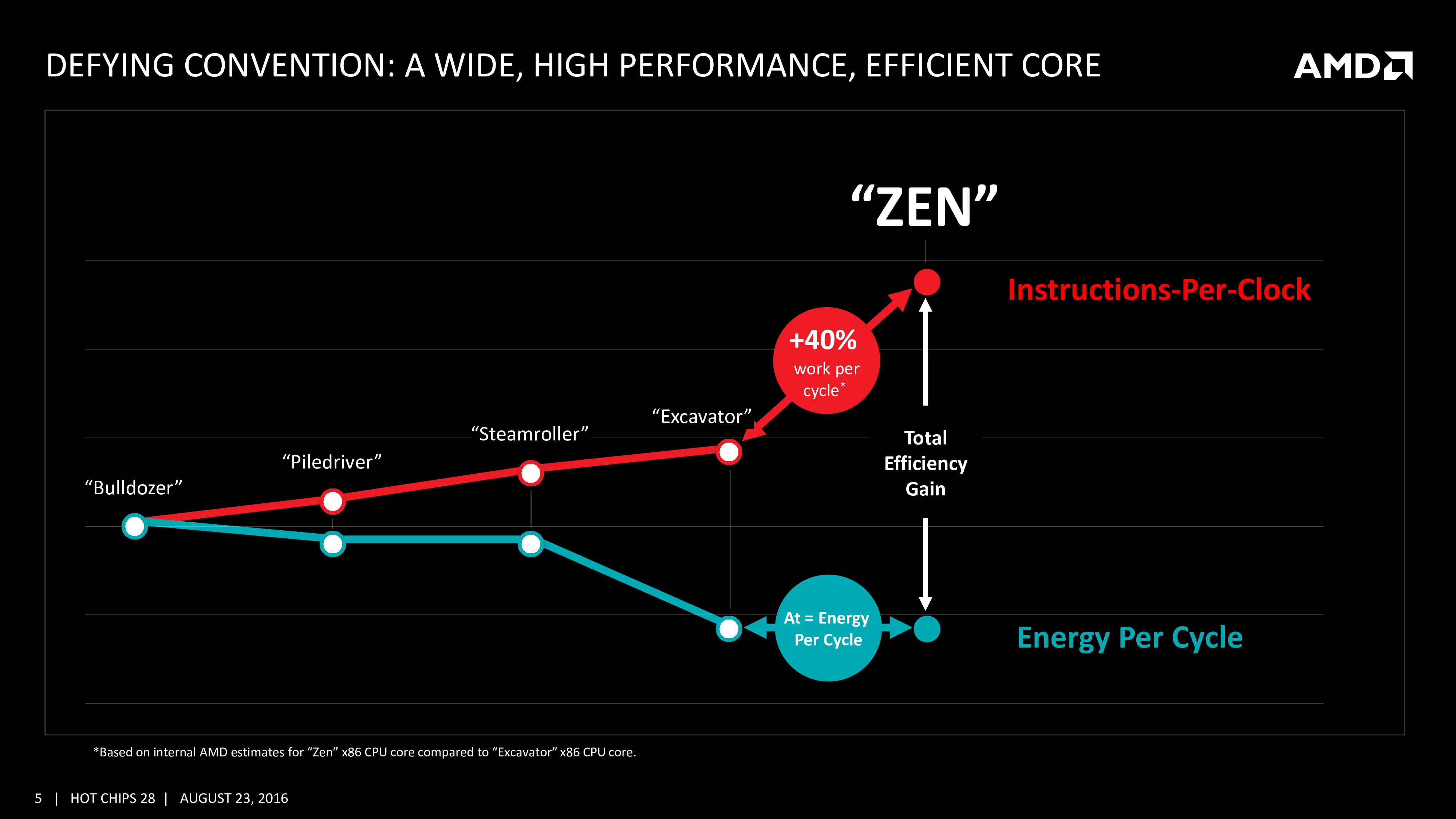
| 22:35, 29 January 2017 | amd zen hc28 page 0004.jpg (file) |  |
473 KB | At32Hz | Slide from AMD's {{amd|Zen|l=arch}} presentation at HC28. | 1 |
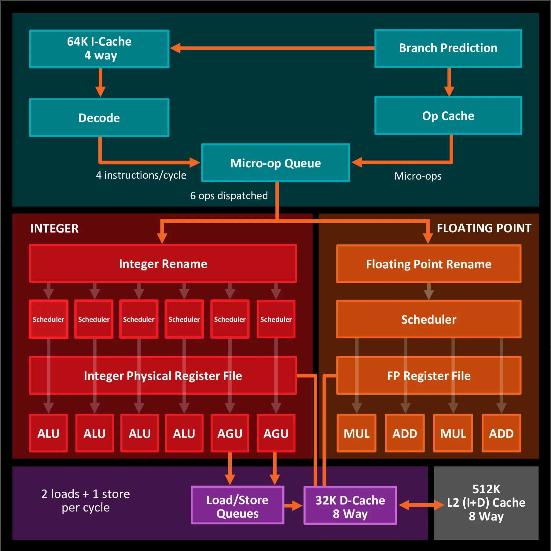
| 22:55, 29 January 2017 | amd zen hc28 overview.png (file) |  |
538 KB | At32Hz | Diagram from AMD's {{amd|Zen|l=arch}} HC28 presentation slide. | 1 |
| 03:06, 30 January 2017 | amd zen hc28 fetch.png (file) |  |
320 KB | At32Hz | AMD {{amd|Zen|l=arch}} front-end fetch overview | 1 |
| 03:44, 30 January 2017 | amd zen hc28 decode.png (file) |  |
303 KB | At32Hz | AMD {{amd|Zen|l=arch}} decode overview slide from HC28 | 1 |
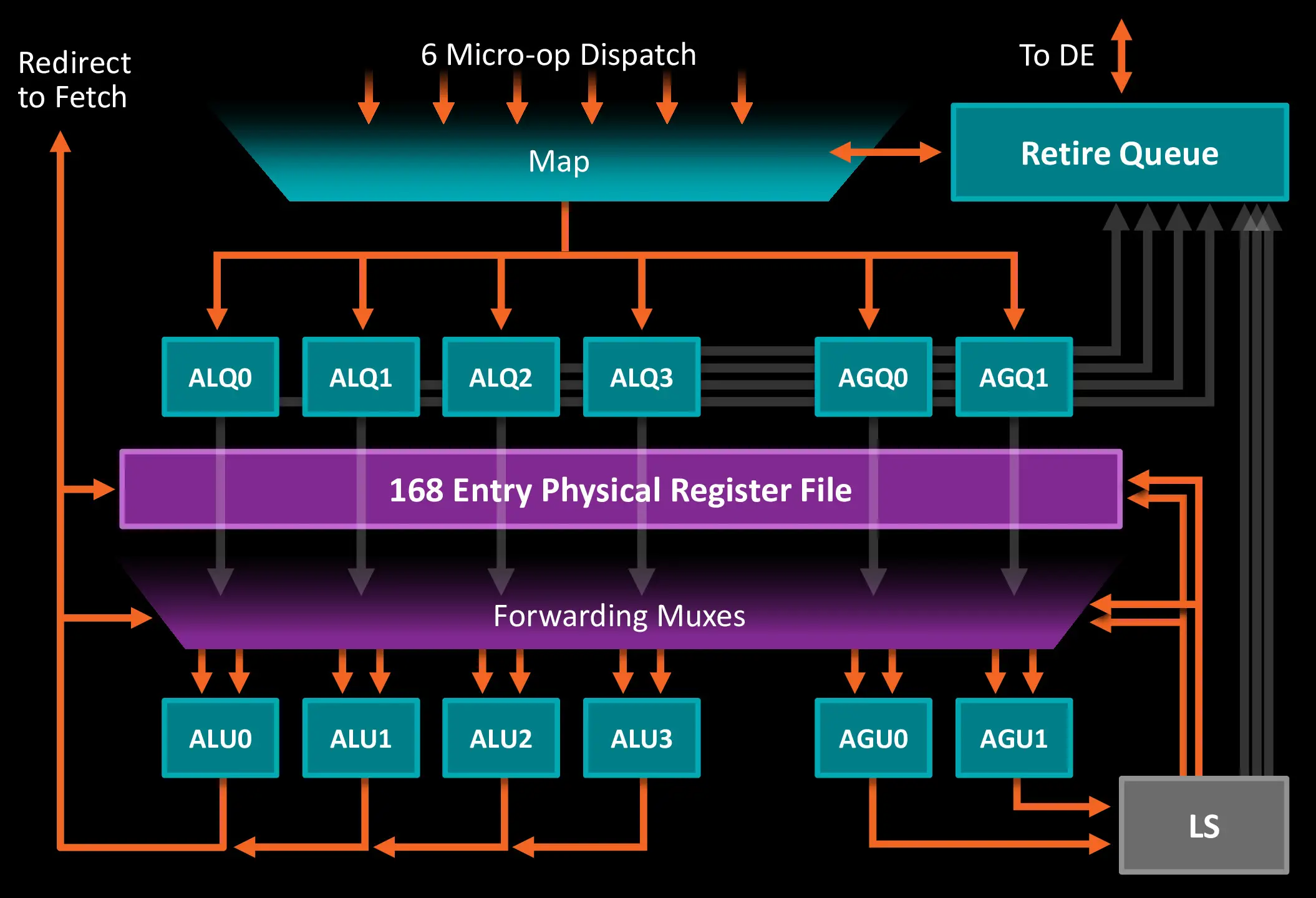
| 21:13, 30 January 2017 | amd zen hc28 integer.png (file) |  |
417 KB | At32Hz | AMD {{amd|Zen|l=arch}} HC28 slide overview of Integer side | 1 |
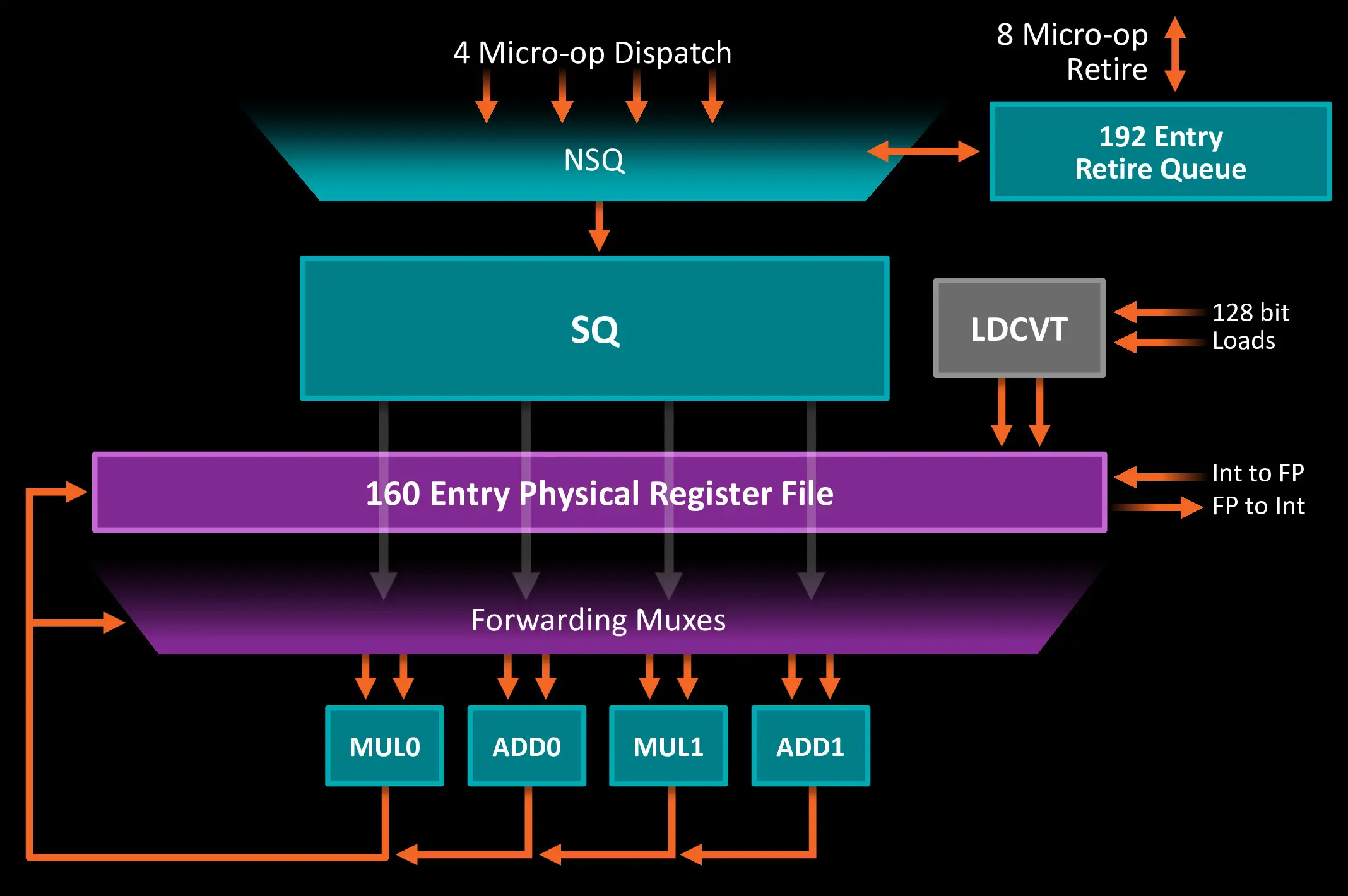
| 21:34, 30 January 2017 | amd zen hc28 fp.png (file) |  |
338 KB | At32Hz | AMD {{amd|Zen|l=arch}} HC28 overview slide of the floating point side. | 1 |
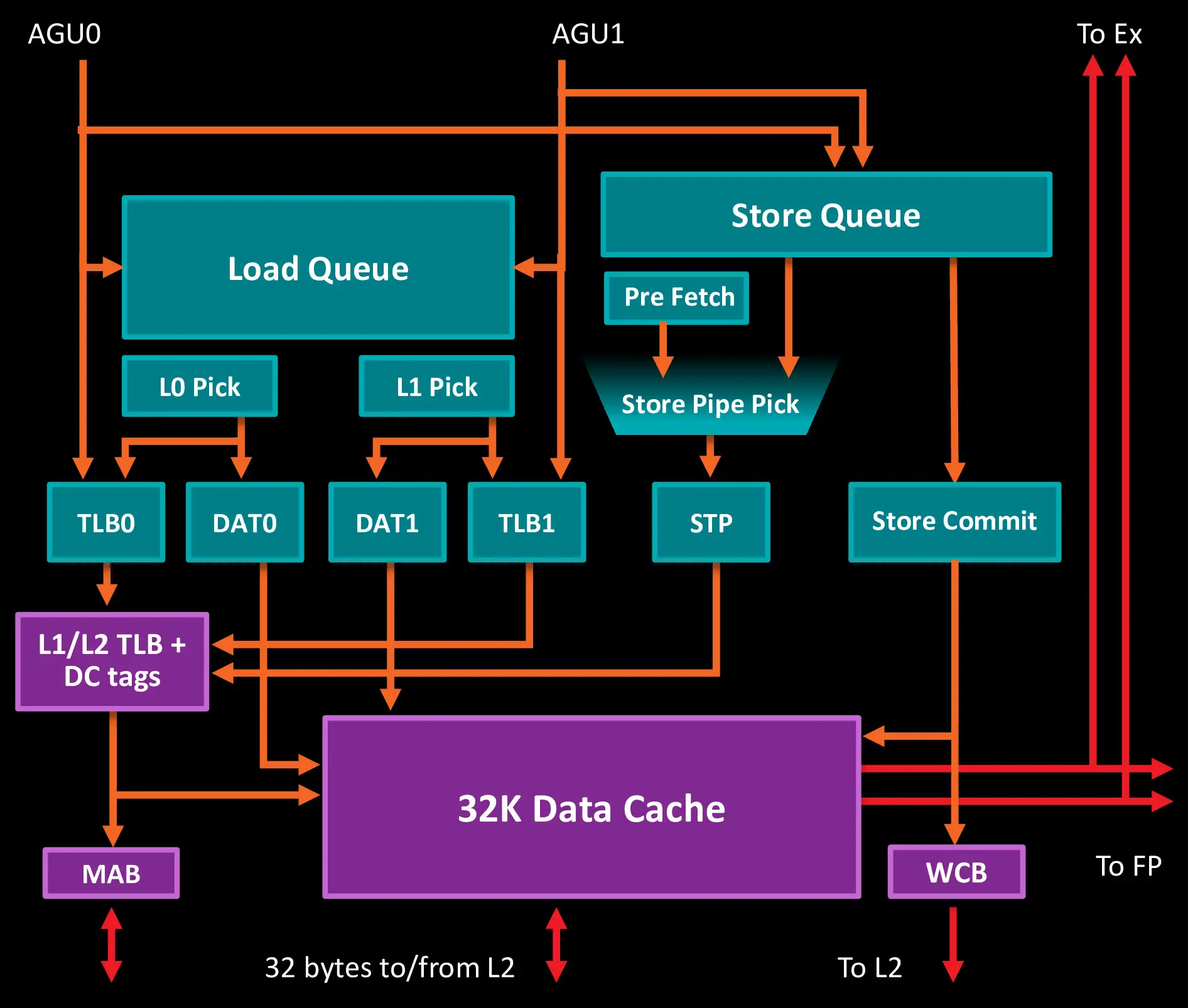
| 22:44, 30 January 2017 | amd zen hc28 memory.png (file) |  |
365 KB | At32Hz | AMD {{amd|Zen|l=arch}} HC28 slide memory overview | 1 |
| 23:23, 30 January 2017 | zen ccx.svg (file) |  |
14 KB | At32Hz | AMD {{amd|Zen|l=arch}} CPU Complex (CCX) | 1 |
| 01:40, 31 January 2017 | amd zen hc28 smt.png (file) |  |
506 KB | ChipIt | AMD {{amd|Zen|l=arch}} SMT overview from HC28 slide | 1 |
| 03:31, 31 January 2017 | 10682-icon-neural-net-prediction-140x140.png (file) | 8 KB | ChipIt | Icon used by AMD for their "Neural Net Prediction" Feature in {{amd|Zen|l=arch}} | 1 | |
| 03:46, 31 January 2017 | 10682-icon-smart-prefetch-140x140.png (file) | 4 KB | ChipIt | Icon used by AMD for their "Smart Prefetch" Feature in {{amd|Zen|l=arch}} | 1 | |
| 03:49, 31 January 2017 | 10682-icon-precision-boost-140x140.png (file) | 6 KB | ChipIt | Icon used by AMD for their "Precision Boost" Feature in {{amd|Zen|l=arch}} | 1 | |
| 03:49, 31 January 2017 | 10682-icon-pure-power-140x140.png (file) | 4 KB | ChipIt | Icon used by AMD for their "Pure Power" Feature in {{amd|Zen|l=arch}} | 1 | |
| 04:12, 31 January 2017 | 10682-icon-frequency-range-140x140.png (file) | 4 KB | ChipIt | Icon used by AMD for their "Extended Frequency Range" Feature in {{amd|Zen|l=arch}} | 1 | |
| 14:22, 31 January 2017 | ibm logo.svg (file) | 5 KB | David | IBM logo | 1 | |
| 14:36, 31 January 2017 | ic logo (ibm).svg (file) | 5 KB | David | IBM IC logo | 1 | |
| 19:56, 4 February 2017 | p9sosmt4.png (file) |  |
31 KB | At32Hz | IBM {{ibm|POWER9|l=arch}} Scale-Out SMT4 from HC28 Presentation | 1 |
| 19:56, 4 February 2017 | p9sosmt8.png (file) |  |
30 KB | At32Hz | IBM {{ibm|POWER9|l=arch}} Scale-Out SMT8 from HC28 Presentation | 1 |
| 19:56, 4 February 2017 | p9susmt4.png (file) |  |
30 KB | At32Hz | IBM {{ibm|POWER9|l=arch}} Scale-Up SMT4 from HC28 Presentation | 1 |
| 19:56, 4 February 2017 | p9susmt8.png (file) |  |
28 KB | At32Hz | IBM {{ibm|POWER9|l=arch}} Scale-Up SMT8 from HC28 Presentation | 1 |
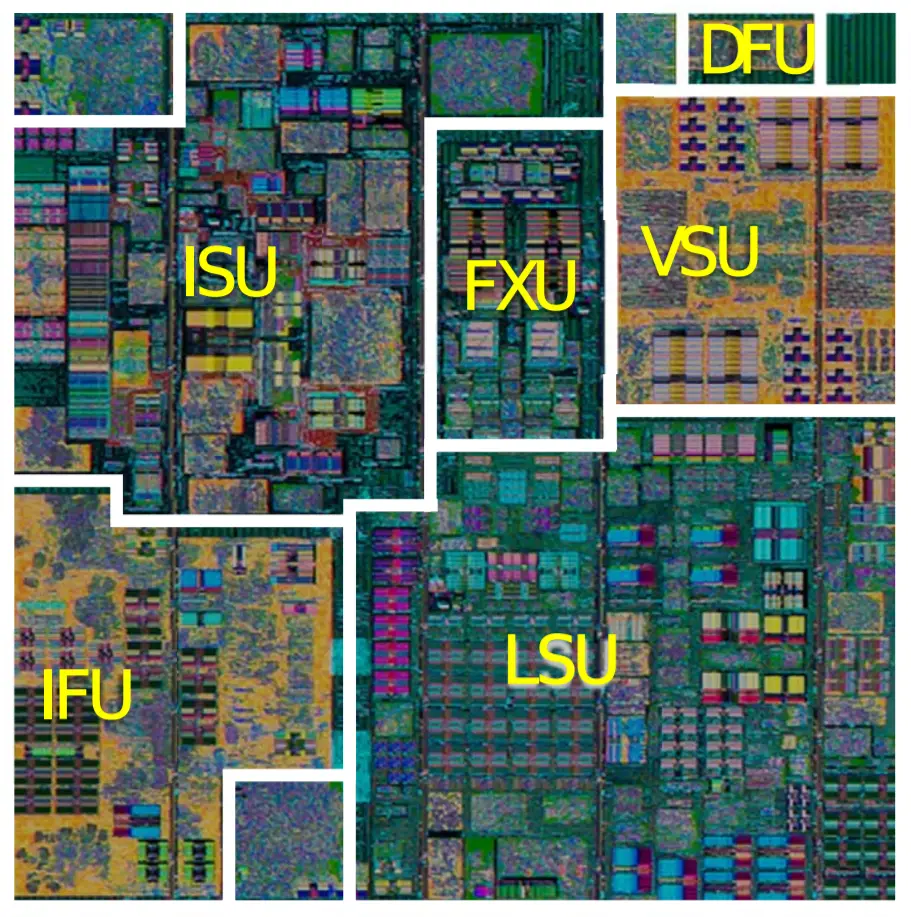
| 22:46, 4 February 2017 | p8smt8comp.png (file) |  |
1.23 MB | At32Hz | IBM {{ibm|POWER8|l=arch}} comp, small size from IBM presentation at HC28. | 1 |
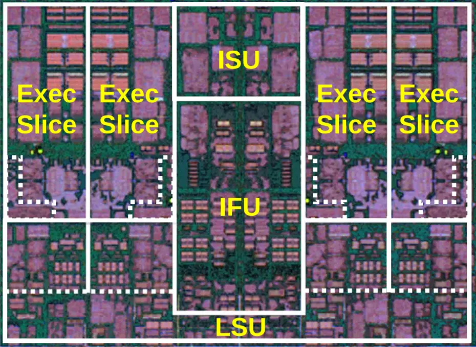
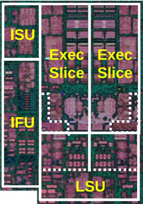
| 22:46, 4 February 2017 | p9slice.png (file) |  |
11 KB | At32Hz | IBM {{ibm|POWER9|l=arch}} Slice from IBM presentation at HC28. | 1 |
| 22:46, 4 February 2017 | p94xsuper-slice.png (file) |  |
925 KB | At32Hz | IBM {{ibm|POWER9|l=arch}} 4x Super-Slice from IBM presentation at HC28. | 1 |
| 22:46, 4 February 2017 | p92xsuper-slice.png (file) |  |
469 KB | At32Hz | IBM {{ibm|POWER9|l=arch}} 2x Super-Slice from IBM presentation at HC28. | 1 |
| 22:46, 4 February 2017 | p9super-slice.png (file) |  |
34 KB | At32Hz | IBM {{ibm|POWER9|l=arch}} Super-Slice from IBM presentation at HC28. | 1 |
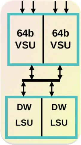
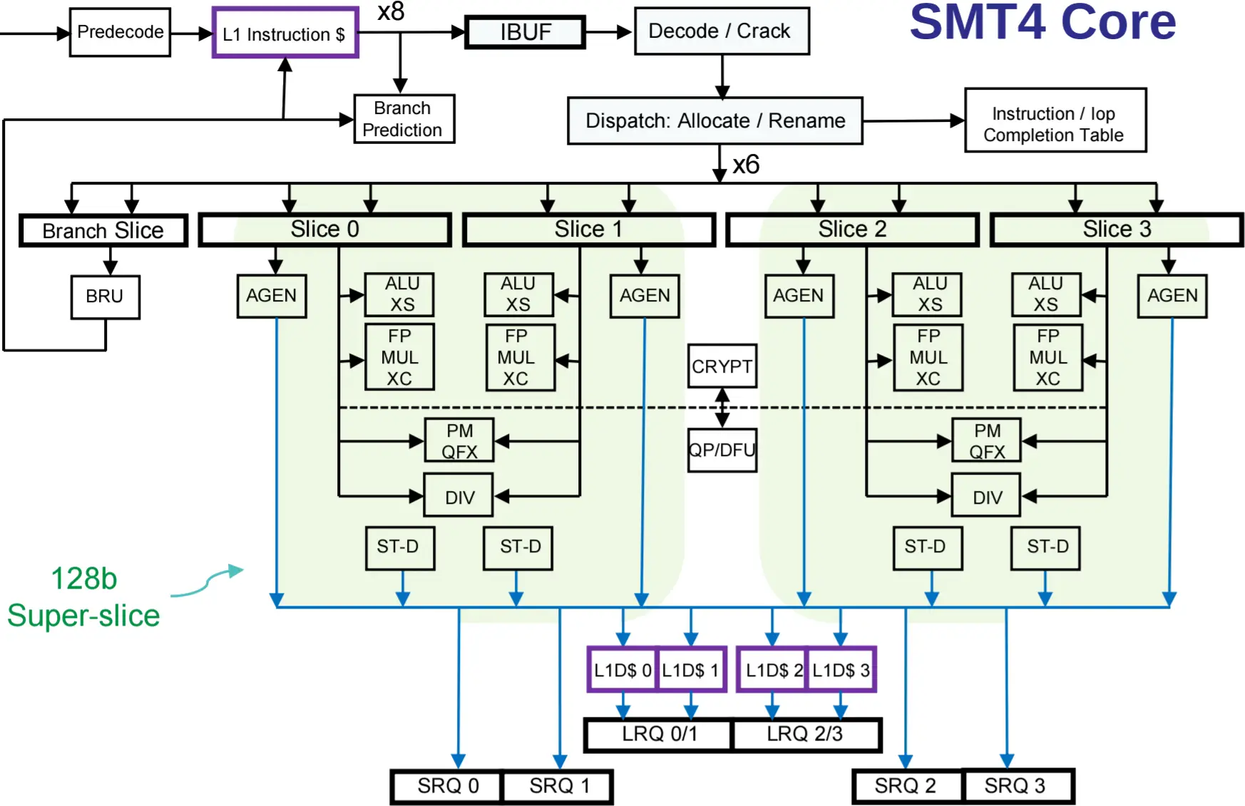
| 23:53, 4 February 2017 | p9smt4core.png (file) |  |
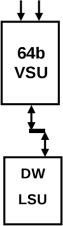
241 KB | At32Hz | IBM {{ibm|POWER9}} SMT4 core | 1 |
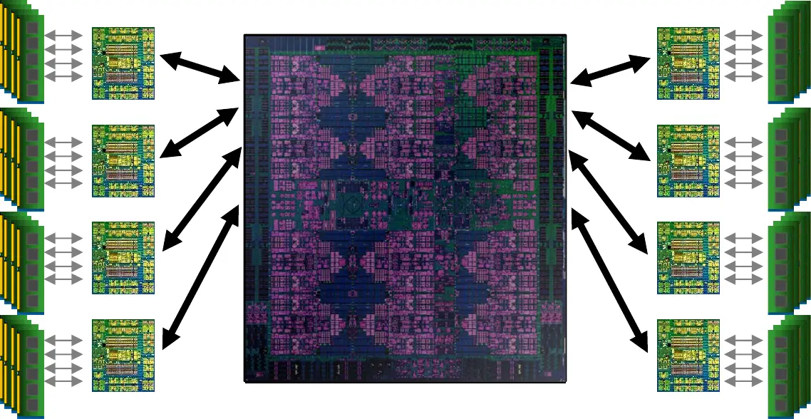
| 01:09, 6 February 2017 | p9somem.png (file) |  |
691 KB | At32Hz | IBM {{ibm|POWER9|l=arch}} Scale-Out Memory | 1 |
| 01:09, 6 February 2017 | p9sumem.png (file) |  |
716 KB | At32Hz | IBM {{ibm|POWER9|l=arch}} Scale-Up Memory | 1 |
| 01:30, 6 February 2017 | p9performance.png (file) |  |
49 KB | At32Hz | IBM {{ibm|POWER9|l=arch}} performance claim slide from HC28. | 1 |
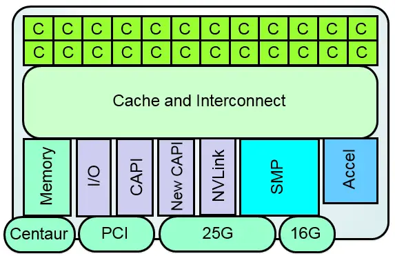
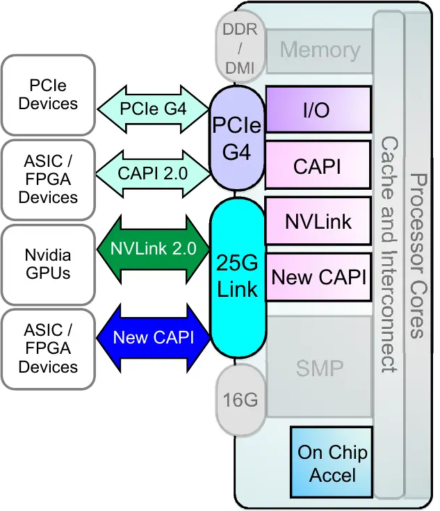
| 04:13, 6 February 2017 | p9links.png (file) |  |
128 KB | At32Hz | IBM {{ibm|POWER9}} links from HC28 IBM presentation | 1 |
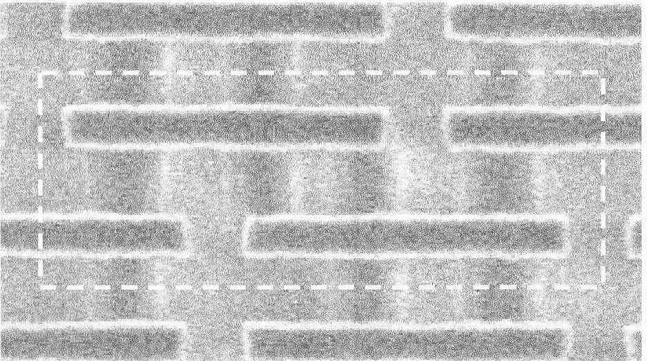
| 09:50, 9 February 2017 | 45nm SRAM Cell.jpg (file) |  |
104 KB | ChipIt | Intel 45 nm 6T SRAM CELL | 1 |
| 10:05, 9 February 2017 | 45nm SRAM photo.JPG (file) |  |
3.41 MB | ChipIt | Die photo of an Intel 45 nm shuttle test chip including 153 MiB SRAM and logic test circuits | 1 |
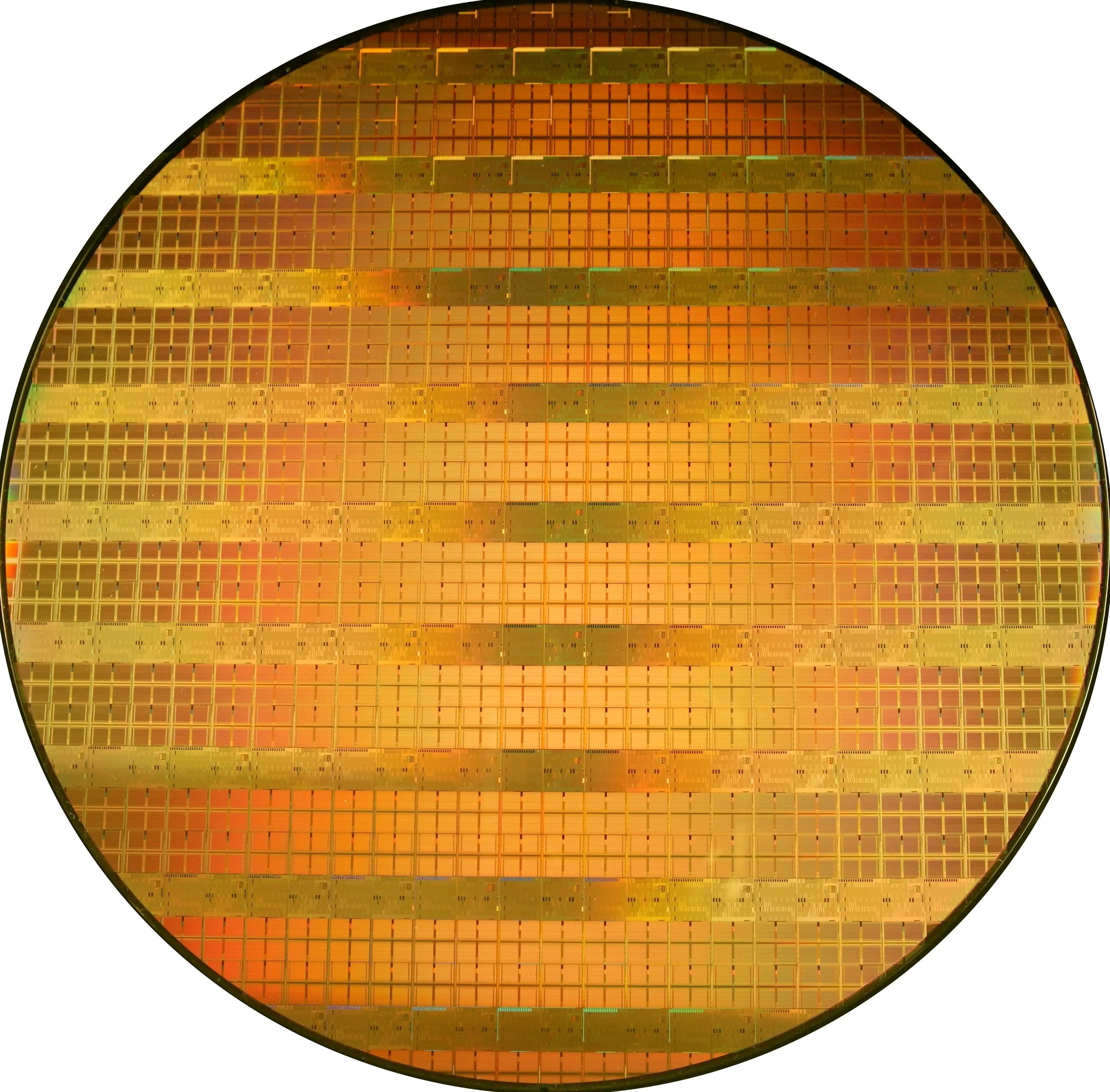
| 10:12, 9 February 2017 | 45nm wafer photo 1.jpg (file) |  |
4.88 MB | ChipIt | Intel 300 mm wafer with 45 nm shuttle test chips | 1 |
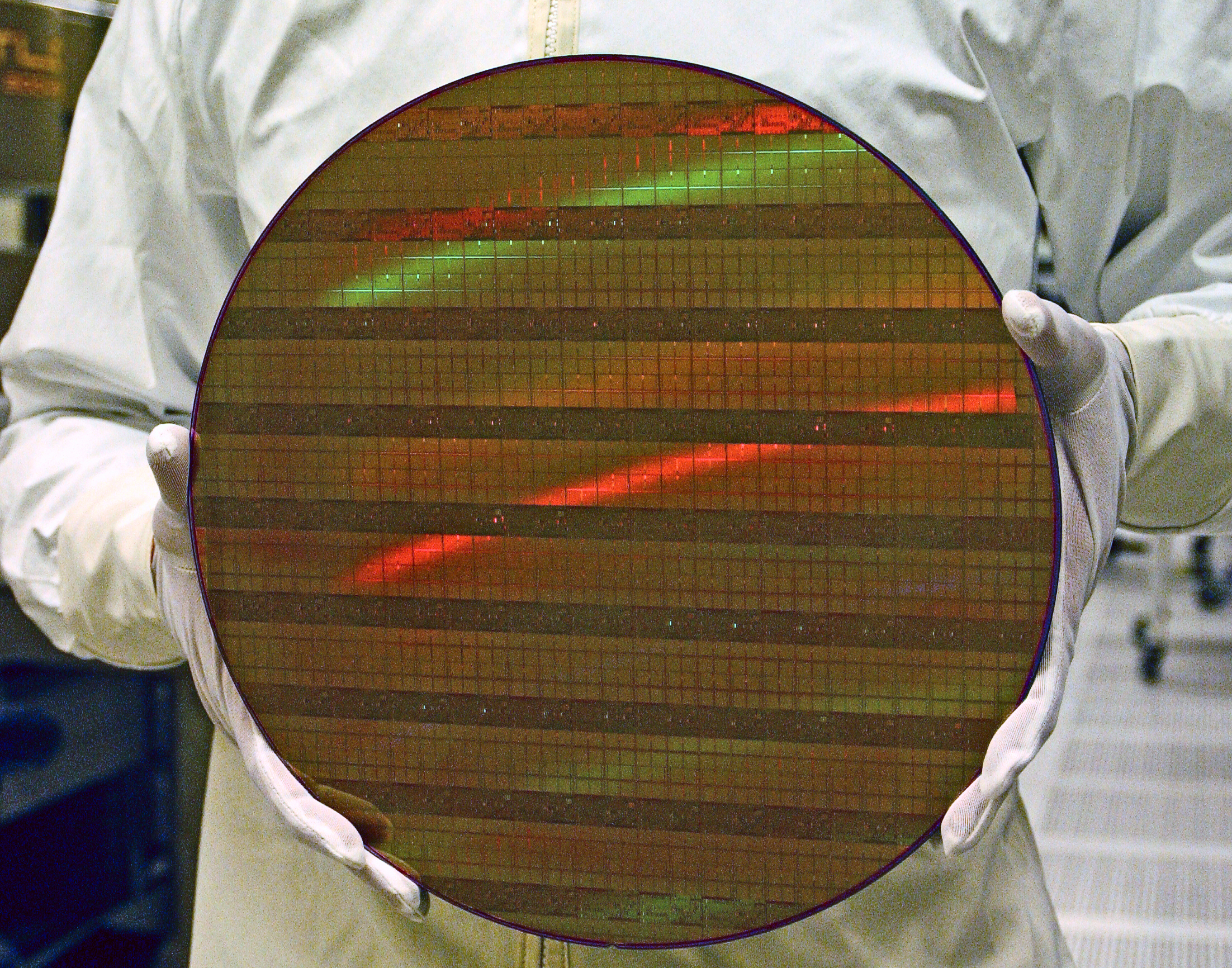
| 10:13, 9 February 2017 | 45nm wafer photo 2.JPG (file) |  |
2.54 MB | ChipIt | Intel engineer holding 300 mm wafer with 45 nm shuttle test chips | 1 |
| 10:13, 9 February 2017 | 45nm-wafer-photo-3.jpg (file) |  |
5.69 MB | ChipIt | Intel 300 mm wafer with 45 nm shuttle test chips | 1 |
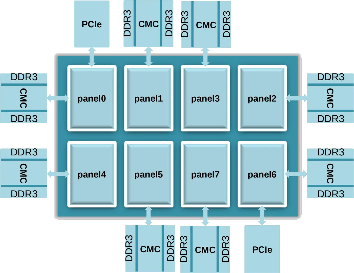
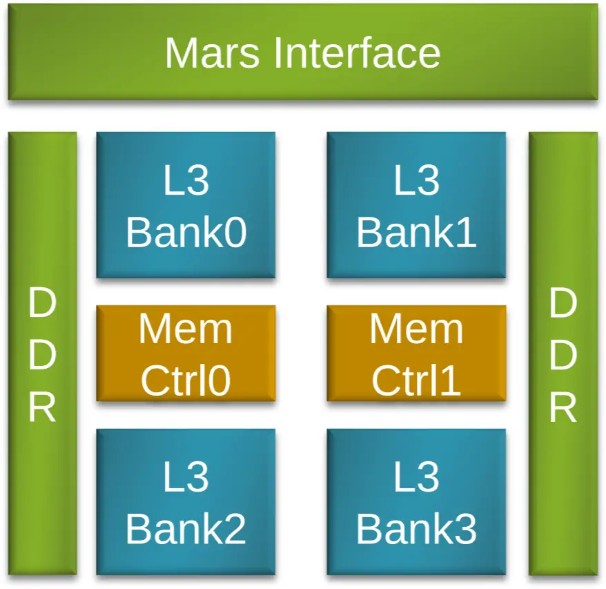
| 00:44, 10 February 2017 | xiaomi panel-based data affinity architecture.png (file) |  |
157 KB | David | Phytium Panel architecture | 1 |
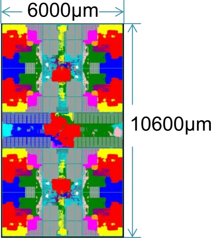
| 01:04, 10 February 2017 | xiaomi panel die (28nm).png (file) | .png) |
447 KB | David | Phytium {{phytium|Xiaomi}} Panel | 1 |
| 01:04, 10 February 2017 | xiaomi panel.png (file) |  |
104 KB | David | Phytium {{phytium|Xiaomi}} Panel | 1 |
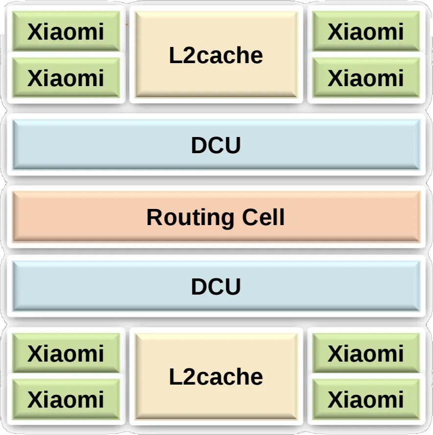
| 21:06, 10 February 2017 | xiaomi block diagram.svg (file) |  |
55 KB | David | 9 | |
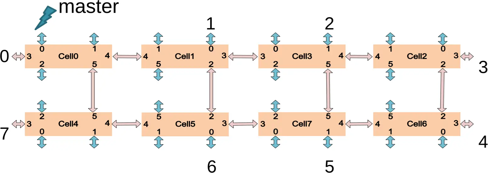
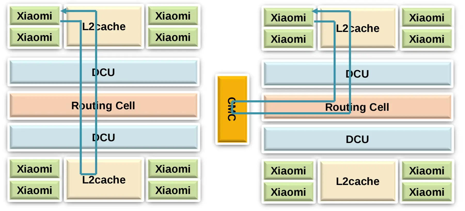
| 23:43, 10 February 2017 | xiaomi 2d network.png (file) |  |
111 KB | David | Phytium {{phytium|Xiaomi}} network | 1 |
| 00:09, 11 February 2017 | xiaomi cmc.png (file) |  |
117 KB | David | Phytium {{phytium|Xiaomi}} CMC chip | 1 |
| 00:51, 11 February 2017 | xiaomi latency.png (file) |  |
202 KB | David | Phytium {{phytium|Xiaomi}} cache flow | 1 |
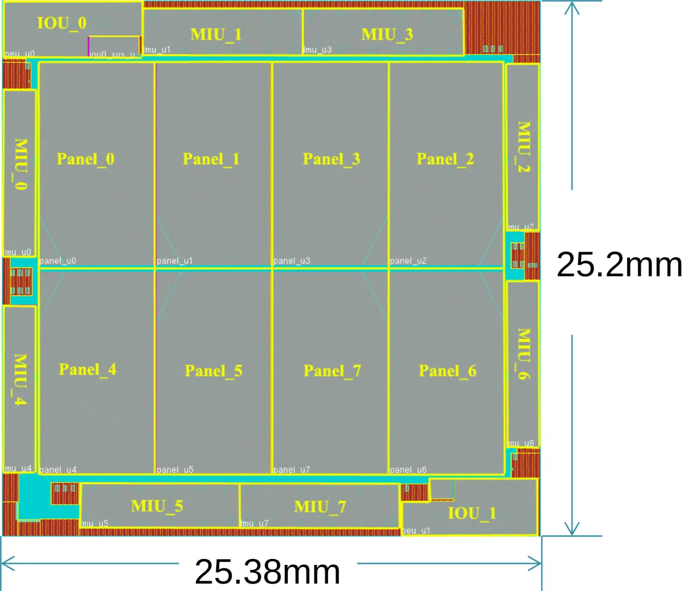
| 01:37, 11 February 2017 | xiaomi floor plan.png (file) |  |
2.58 MB | David | Phytium {{phytium|Xiaomi}} floor plan | 1 |
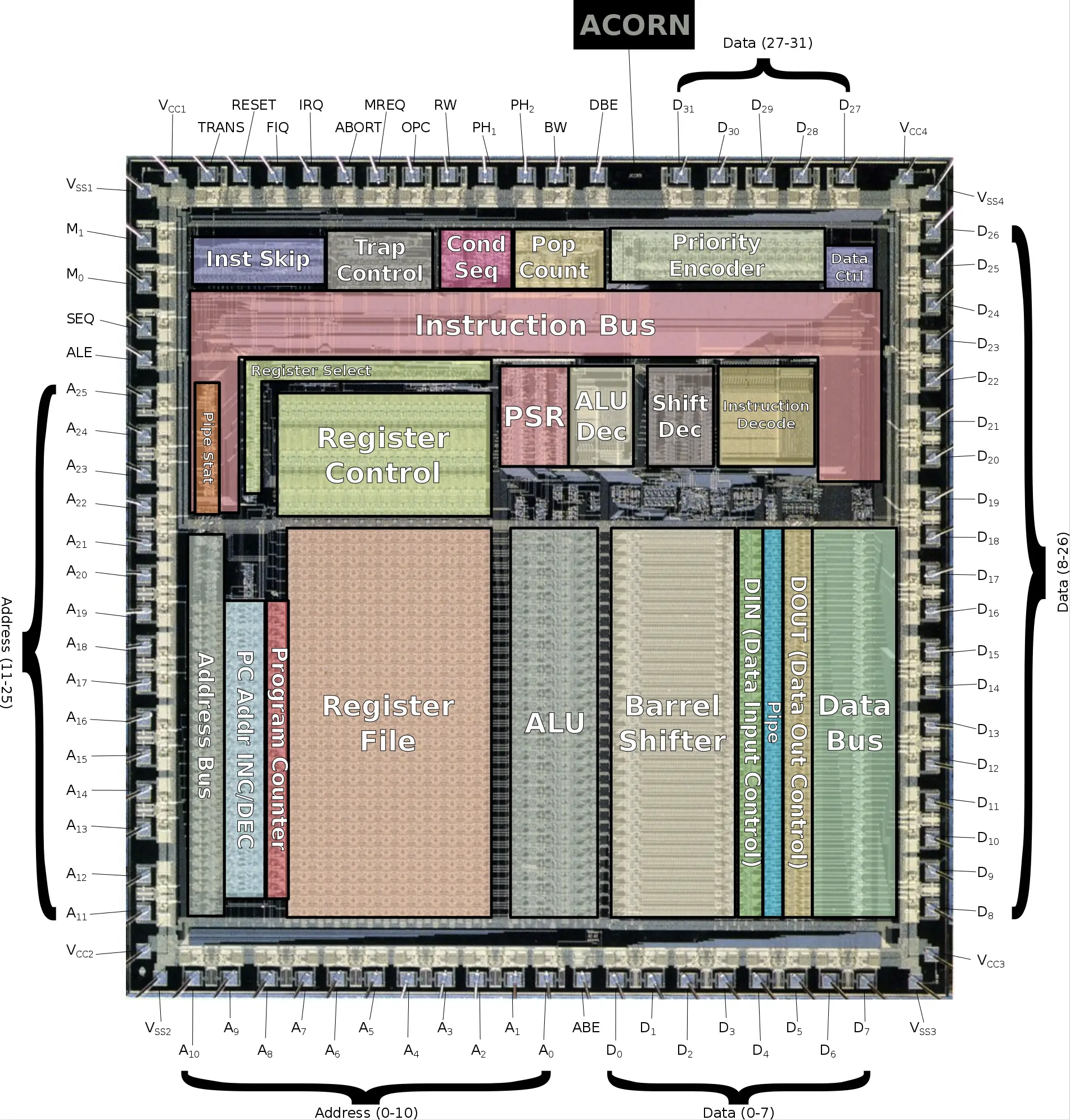
| 18:07, 12 February 2017 | arm1 die shot (annotated).png (file) | .png) |
3.68 MB | ChipIt | WikiChip annotation of the ARM1 die shot by ARM Ltd. * Original @ File:arm1_die_shot.png | 1 |
.svg)
First page |
Previous page |
Next page |
Last page |