Nanotube-RAM (NRAM) is a carbon nanotube-based resistance-change memory-class storage RAM. NRAM is proprietary technology developed by Nantero licenseable to manufacturers.
Overview[edit]
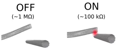
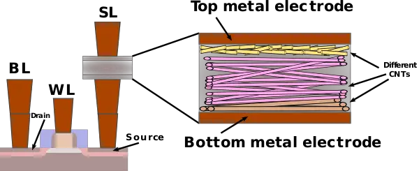
NRAM uses carbon nanotubes (CNTs) as the switching medium situated between two electrodes located in the BEOL. The underlying device and substrate need not matter. It is resistance-change memory meaning an "off" state is a result of high resistance while an "on" state is a result of low resistance. The resistance of the bit cell is determined by the contact arrangement of the stochastic fabric of CNTs. When a sufficient amount of CNTs are touching each other, the overall resistance of the network of disordered CNTs is low, on the order of 100 kΩ. Likewise, when disconnected, the overall resistance of the network is very high, on the order of 1 MΩ. NRAM relies on the van der Waals force to keep CNTs bound to each other as well as apart.
Technology[edit]
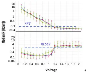
A typical NRAM cell consists of a non-woven fabric of hundred to thousand of carbon nanotubes (CNTs). NRAM relies on the basic principle of the van der Waals force which is used to keep the CNTs attractive once they are connected and repulsive when they are apart. Their repulsive and adhesive behavior is a function of the van der Waals distance. An electrostatic force is needed to overcome their repulsion and connect them. Once connect the tubes will remain connected until an electrostatic force of the opposite charge breaks them apart. Therefore the entire NRAM bit cell forms a stochastic array of resistive elements. An electrostatic force is used to combine a sufficiently large amount of CNTs to lower the resistance and an opposite force is used to break them apart to significantly increase the resistance. An NRAM cell is a dielectric-free cell which has shown no wear-out.
An NRAM cell is largely device-agnostic (both process-agnostic and transistor-agnostic) as well as substrate-agnostic. Once the FEOL devices are fabricated, metal contacts in the BEOL are exposed where desired. A pure carbon nanotube slurry is then spin coated on top of those structures in order to form a uniform layer which is then followed by a bake and a top metal.
It's worth noting that the CNTs forming the top and bottom parameter of the cell (in particular, the CNTs just below the top metal) do not move. Those have a protective barrier in order to permanently fix them to their location, preventing the top metal from slowly permeating its way into the cell and shorting it. Most of the CNTs participating in the storage (i.e., creating the resistance) are taken from the bottom. Those CNTs are pulled up in order to create a void and increase the resistance and are then forced back down in order to lower the resistance. Both the length and the diameter of the carbon nanotubes is carefully chosen depending on the attributes of the NRAM cell used. CNTs that are too long will simply short the cell. Likewise, CNTs that are too short can stand up and not switch either. Therefore it is important that the CNTs are in a specific range suitable for the specific NRAM.
Characteristics[edit]
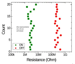
NRAM is non-volatile, retaining its state without power. Under typical operating temperature (~110-140 °C), NRAM is reported to have a data retention of around 12,000 years. Under worse operating temperatures (-55 °C or 300 °C), data retention remains well over 300 years (likely over 1,000 years). There is great potential for radiation hardness due to its immunity to alpha particles. The difference between 0 and 1 is greater than 10X in the resistance between the two electrodes. This makes detection relatively simple and no complex process controls and extra calibrations across the wafer.
NRAM has a 3-5ns read/write access time, making it significantly faster than DRAM and even a viable last level cache. It's worth noting that writes are faster than reads. From a power perspective, NRAM consumes around 4-5 fJ/bit, slightly better than DRAM (5-7 fJ/bit). Additionally, since there is no capacitors involved, no refresh is necessary therefore the effective bandwidth over comparable DRAM products is higher.
For this reason, NRAM offers an attractive forward scaling path beyond what DRAM can deliver. Though it would appear that DRAM should scale similarly to NRAM, in practice there is a minimum size at which DRAM can be designed. Below that size, the storage capacitor is not capable of storing enough charge. NRAM, on the other hand, keeps its state in terms of resistance levels meaning it's limited only by lithography. Scaling down to 5 nm is well understood and it is thought that NRAM can scale down to a 1 nm process.
Scaling[edit]
There are a number of ways in which NRAM can scale. Process scaling is largely a function of the number of CNTs per bit. Switching is well understood with just a few 100s CNTs, therefore, NRAM can scale down to well below the 5 nm process. In addition to traditional lithography scaling, since NRAM is embedded into the BEOL, it can be built right on top of memory or logic (e.g., NRAM on top of a CPU core) or even analog (in fact the type of device does not matter). It's worth noting that this can actually be repeated as many times as desired, forming multiple layers vertically. As with other technologies, NRAM can also be scaled through TSVs and die stacking. Although Nantero did not fully disclose the specifics, NRAM can be further scaled in terms of density through the use of multi-level cells as a function of the pulse.
Bibliography[edit]
- Gervasi, Bill, Nantero Principal Systems Architect (September 14, 2018). Personal interview.
- IEEE Hot Chips 30 Symposium (HCS) 2018


