Semiconductor & Computer Engineering
| Edit Values | |
| Loihi | |
 | |
| General Info | |
| Designer | Intel |
| Manufacturer | Intel |
| Market | Artificial Intelligence |
| Introduction | September 25, 2017 (announced) January, 2018 (launched) |
| Shop | Amazon |
| Neuromorphic Specs | |
| Neurons | 131,072 |
| Synapses | 130,000,000 |
| Microarchitecture | |
| Process | 14 nm |
| Transistors | 2,070,000,000 |
| Technology | CMOS |
| Die | 60 mm² |
| Multiprocessing | |
| Max SMP | 16,384-Way (Multiprocessor) |
| Vcore | 0.50 V-1.25 V |
| Packaging | |
 | |
| Succession | |
Loihi (pronounced low-ee-hee) is a neuromorphic research test chip designed by Intel Labs that uses an asynchronous spiking neural network (SNN) to implement adaptive self-modifying event-driven fine-grained parallel computations used to implement learning and inference with high efficiency. The chip is a 128-neuromorphic cores many-core IC fabricated on Intel's 14 nm process and features a unique programmable microcode learning engine for on-chip SNN training. The chip was formally presented at the 2018 Neuro Inspired Computational Elements (NICE) workshop in Oregon.
The chip is named after the Loihi volcano as a play-on-words - Loihi is an emerging Hawaiian submarine volcano that is set to surface one day.
Loihi was succeeded by Loihi 2 in late 2021.
Contents
Overview[edit]
Announced in September 2017, Loihi is predominantly a research chip meaning performance characteristics are not guaranteed. This is Intel's 5th chip in the neuromorphic category. The first three chips were early internal test chips while the fourth is a 10 nm wafer-level probe study. Loihi consists of an asynchronous spiking neural network (SNN) meaning instead of manipulating signals, the chip sends spikes along activate synapses. Connections are asynchronous and highly timed based. Neuromorphic cores containing many neurons are interlinked and receive spikes from elsewhere in the network. When received spikes accumulate for a certain period of time and reach a set threshold, the core will fire off its own spikes to its connected neurons. Preceding spikes reinforce each other and the neuron connections while spikes that follow will inhibit the connection, declining the connectivity until all activities are halted.
The chip was initially tested and simulated using FPGAs. Actual silicon implementations arrived in late November.
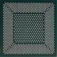
Loihi is fabricated on Intel's 14 nm process and has a total of 130,000 artificial neurons and 130 million synapses. In addition to the 128 neuromorphic cores, there are 3 managing Lakemont cores.
Architecture[edit]

The chip consists of a many-core mesh of 128 neuromorphic cores, three Lakemont x86 cores (Quark), and an off-chip communication interface that allows the chip to scale out to many other chips in the four planar directions (as shown on the right). The implemented mesh protocol supports up to 4,096 on-chip cores and up to 16,384 chips.
The chip itself implements a fully asynchronous many-core mesh of 128 neuromorphic cores. It implements a spiking neural network (SNN) whereby at any given time one or more of the implemented neurons may send out an impulse (i.e., spike) to its neighbors through the directed links (synapses). All neurons have a local state with their own set of rules that affects their evolution and the timing of spike generation. Interaction is entirely asynchronous, sporadic, and independent of any other neuron on the network. A unique feature of Loihi's neuromorphic cores is their integrated learning engine which enables full on-chip learning via programmable microcode learning rules.
Core-to-core communication is done in using packetized messages with write, read request, and read response messages for core management and x86-to-x86 messaging, spike messages, and barrier messages (for synchronization).
Neuromorphic Core[edit]
Loihi implements 128 neuromorphic cores, each containing 1,024 primitive spiking neural units grouped into tree-like structures in order to simplify the implementation. Each of those groups shares the same fan-in and fan-out connections, configuration, and state variables in ten architectural memories.

Above is the block diagram of the major memory blocks where the various connectivities, configurations, and dynamic states of all the neurons that are mapped to the neuromorphic core. Each core incorporates a total of 2 Mib (including ECC). Spikes are received on the input side, handled internally (synaptic/group update), and a spike is optionally generated in the output if the various conditions are met. For the most part, those blocks operate independently with little control synchronization. Intel has parallelized the hardware where a single large event can be handled more efficiently as a few smaller events. This is shown as a dotted line. One example Intel provided is extracting synapses from the memory and to the dendrite accumulator through the modification and even the learning engine is with up to four-way parallelism. In addition to the normal flow, there's the configurable learning engine shown under the major blocks (described below).
Loihi implements a variant of the current-based synapse (CUBA) leaky integrate-and-fire neuron model with two internal state variables:
- Synaptic response current - the weighted sum of the input spikes and a constant bias
- Membrane potential - a leaky (i.e. weakens over time) spike potential function that sends out a spike when the potential passes the firing threshold
It's worth noting that since Loihi is a digital architecture, the above continuous functions are approximated using a discrete timestep whereby all neurons maintain a timestamp synchronized throughout the entire chip. This is needed in order to enable well-defined behaviors.
Operation and Communication[edit]

The operation itself is fairly straightforward, once enough spikes accumulate and exceed the predefined threshold level, a spike message is created and sent out to various other groups in various destination cores. Loihi is actually the first neuromorphic chip to feature a fully integrated SNN meaning it can support unicast, multicast, broadcast, sparse network, variable synaptic formats (any weight precision 1-9 bits, +/-, etc..), and population-based hierarchical connectivity.
Communication is done by each of the cores independently iterating over each of their neuron groups and for every group that enters a firing state, the core generates a spike message that is distributed to all the other cores on the mesh that contain their synaptic fanouts. The iterations of all the groups by all the cores must be done within the same discrete timestamp. To ensure that all the spikes have made it to their destinations before the operation is repeated, Loihi sends out a synchronization message whereby any spikes in-flight are flushed in the first phase and in the second phase a timestep-advance notification is sent to all the cores to advance their timestamp to , enabling them to proceed to update their internal groups.
It should be noted that Loihi supports a hierarchical network model which means it can exploit the localized sub-networks in the mesh in order to substantially reduce the chip-wide connectivity and synaptic resources required to map the networks.
Self-learning[edit]
Each core contains a "learning engine" (marked in the block diagram above as 'learning') that can be programmed to adapt to the network parameters during operation such as the spike timings and their impact. It does this by updating the synaptic weights using the 4-bit microcode-programmed learning rules that are specifically associated with that synapse. Updates (or 'learning') is done at each learning epoch, a period of time that is globally preconfigured per core. This makes the chip more flexible as it allows various paradigms such as supervisor/non-supervisor and reinforcing/reconfigurability without requiring any particular approach. The choice for higher flexibility is intentional in order to defer various architectural decisions that could be detrimental to research.
Programming[edit]
Intel has developed a complete toolchain for working with Loihi including a Loihi Python API, a compiler, and a set of runtime libraries for building and executing SNNs on Loihi. For the most part, the API is similar to existing frameworks such as PyNN. The Loihi API provides a way of creating a graph of neurons and synapses with custom configurations such as decay time, synaptic weight, and spiking thresholds. The graphs can then be stimulated by injecting external spikes and learn through custom learning rules.
Loihi-based neuromorphic system[edit]
Intel developed a series of systems based on Loihi which scale to a large number of Neurons and Synapses.
| Kapoho Bay | Wolf Mountain | Nahuku | Pohoiki Beach | Pohoiki Springs |
|---|---|---|---|---|
| USB FF | Board | FPGA Expansion Card | Multi-Board System | Many-Board System |
| 1-2 Chips | 4 Chips | 8 - 32 Chips | 64 Chips | 768 Chips |
| 130,000,000 - 260,000,000 Synapses | 520,000,000 Synapses | 1,040,000,000 - 4,160,000,000 Synapses | 8,320,000,000 Synapses | 99,840,000,000 Synapses |
| 131,072 - 262,144 Neurons | 524,288 Neurons | 1,048,576 - 4,194,304 Neurons | 8,388,608 Neurons | 100,663,296 Neurons |
Kapoho Bay (2 chip, 262K neurons)[edit]
Kapoho Bay is a USB stick form factor that incorporates 1 or 2 Loihi chips. Announced on Dec 6, 2018, Kapoho Bay includes a USB host interface and a DVS interface for neuromorphic sensors such as a camera. With 2 chip Kapoho Bay has 256 neuromorphic cores with 262,144 neurons and 260,000,000 synapses.

Wolf Mountain (4 chip, 524K neurons)[edit]
Wolf Mountain was the first research board that shipped to researchers. This board incorporated four chips for a total of 512 neuromorphic cores meaning 524,288 neurons and 520,000,000 synapses.

Nahuku (32 chip, 4M neurons)[edit]
Nahuku is a scalable Arria10 FPGA expansion board. Intel uses the Nahuku board as the framework for building larger systems. The Nahuku board comes in multiple configurations from 8 to 32 chips. Those chips are organized as 16 chips in a 4 by 4 grid mesh on both sides. With 32 chips there is a total of 4,096 neuromorphic cores incorporating a total of 4,194,304 neurons and 4,160,000,000 synapses. With the Nahuku board, an FPGA host is connected to a set of conventional sensors such as actuators as well as neuromorphic sensors such as a DVS camera or a silicon cochlea. The board communicates with a standard "super host" CPU which can be used to send commands to the board and to the management core on the chips themselves.

Pohoiki Beach (64 chip, 8M neurons)[edit]
Pohoiki Beach is a scaled up system comprising two Nahuku boards for a total of 64 chips. With 64 chips there is a total of 8,192 neuromorphic cores incorporating a total of 8,388,608 neurons and 8,320,000,000 synapses.
Pohoiki Springs (768 chip, 100M neurons)[edit]
Pohoiki Springs is a very large scale system that consists of 24 Nahuku boards for a total of 768 Loihi chips. This system contains 8 rows with 3 slots each for 3 boards per row and eight rows for a total of 24 boards. With 24 boards in the system, there is a total of 768 chips for a total of 98,304 neuromorphic cores incorporating a total of 100,663,296 neurons and 99,840,000,000 synapses.

Die[edit]

- 14 nm process
- 2,070,000,000 transistors
- 128 neuromorphic cores + 3 x86 cores
- 60 mm² die size
- Core area 0.41 mm²
- Density
- 2,184 neurons per mm²
- 2.1 million unique synaptic variables per mm²

Bibliography[edit]
- Some information was obtained directly from Intel
- Jim Held, Intel Fellow & Director Emerging Technologies Research, Intel Labs, HPC Developer Conference 2017 ("Leading The Evolution of Compute: Neuromorphic and Quantum Computing").
- Davies, Mike, et al. "Loihi: A Neuromorphic Manycore Processor with On-Chip Learning." IEEE Micro (2018).
See also[edit]
| back image | .png) + + |
| core voltage (max) | 1.25 V (12.5 dV, 125 cV, 1,250 mV) + |
| core voltage (min) | 0.5 V (5 dV, 50 cV, 500 mV) + |
| designer | Intel + |
| die area | 60 mm² (0.093 in², 0.6 cm², 60,000,000 µm²) + |
| first announced | September 25, 2017 + |
| first launched | January 2018 + |
| full page name | intel/loihi + |
| instance of | neuromorphic chip + |
| ldate | January 2018 + |
| main image | .png) + + |
| manufacturer | Intel + |
| market segment | Artificial Intelligence + |
| max cpu count | 16,384 + |
| name | Loihi + |
| neuron count | 131,072 + |
| process | 14 nm (0.014 μm, 1.4e-5 mm) + |
| smp max ways | 16,384 + |
| synapse count | 130,000,000 + |
| technology | CMOS + |
| transistor count | 2,070,000,000 + |
.png)
.png)