| Edit Values | |
| z15 µarch | |
| General Info | |
| Arch Type | CPU |
| Designer | IBM |
| Manufacturer | GlobalFoundries |
| Introduction | September 12, 2019 |
| Process | 14 nm |
| Core Configs | 9, 10, 11, 12 |
| Pipeline | |
| Type | Superscalar, Pipelined |
| OoOE | Yes |
| Speculative | Yes |
| Reg Renaming | Yes |
| Stages | 17 |
| Decode | 6-way |
| Instructions | |
| ISA | z/Architecture |
| Cache | |
| L1I Cache | 128 KiB/core 8-way set associative |
| L1D Cache | 128 KiB/core 8-way set associative |
| L3 Cache | 256 MiB/chip 32-way set associative |
| L4 Cache | 960 MiB/drawer 60-way set associative |
| Succession | |
z15 is the successor to the z14, a 14 nm z/Architecture mainframe microarchitecture designed by IBM and introduced in 2019.
Contents
Process Technology[edit]
IBM fabricates its z15 microprocessors and system controllers on GlobalFoundries's 14 nm (14HP) FinFET Silicon-On-Insulator (SOI) process featuring highly-dense deep trench structures used for high-density eDRAM.
Release Dates[edit]
The z15 was launched by IBM on September 12, 2019. General availability of the z15 mainframe started September 23.
Architecture[edit]
Key changes from z14[edit]
- Mainframe
- Up to 190-way multiprocessing (from 170-way)
- Less CPs per drawer (4, down from 6)
- Less CPs per logical cluster (2, down from 3)
- 1 more drawer (5, up from 4)
- 0-12 PCIe+ I/O drawers (up from 0-5 drawers)
- Rack
- standard 19" racks (from 24-inch racks)
- 1-4 frame configs (up from only 2-frame configs)
- rear only I/O and power connections (from front & rear)
- Central Processor (CP)
- 2 more cores (12, up from 10)
- Core
- 10-13% higher IPC (IBM claim)
- Front-end
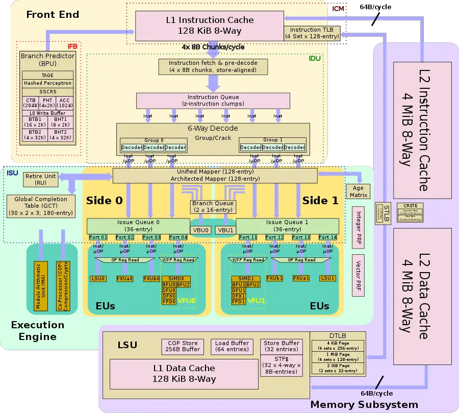
- Improved branch predictor
- New TAGE predictor
- BTB pre-buffer (BTBp) replaced by a simpler write buffer
- single double-bandwidth port (two independentread ports)
- 2x larger L1 BTB (8 sets of 2K rows, up from 4 sets of 2K rows)
- Improved branch predictor
- Back-end
- Larger GCT (60 groups, up from 48 groups)
- Wider retire (12 instructions/cycle, up from 10)
- Larger Issue Queues (2 x 36-entry, up from 2 x 30-entry)
- 2x larger mapper (128-entry, up from 64-entry)
- Larger integer physical register files (???, up from 120 entries)
- Larger vector physical register files (???, up from 127 entries)
- Larger GCT (60 groups, up from 48 groups)
- Execution engine
- Wider execute (12 instructions/cycle, up from 10)
- New Modulo Arithmetic (MA) unit
- Memory subsystem
- 2x larger L2 instruction cache (4 MiB, up from 2 MiB)
- 2x larger 2 GiB pages STLB (256-entry, up from 64 entries)
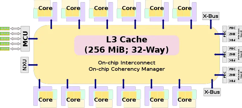
- Shared L3
- 2x larger L3 (256 MiB, up from 128 MiB)
- I/O
- GX Bus removed
- X Bus removed (2 interface, down from 3)
- New PCIe Gen interface (3 interfaces, up from 2)
- Memory
- Larger memory support (40 TiB, up from 32 TiB)
- New integration
- Nest Acceleration Unit (NXU)
- System Controller (SC)
- 1.4x Larger L4 cache (960 MiB, up from 672 MiB)
- Non-exclusive (from inclusive)
- 1.4x Larger L4 cache (960 MiB, up from 672 MiB)
Block Diagram[edit]
CP Chip[edit]
Individual core[edit]
Memory Hierarchy[edit]
The z15 features a memory structure very similar to the z14.
- Cache:
- L1 instruction cache
- 128 KiB, 8-way set associative
- 64 sets, 256 B line size
- L1 data cache
- 128 KiB, 8-way set associative
- 64 sets, 256 B line size
- L2 instruction cache
- 4 MiB, 8-way set associative
- 2K sets, 256 B line size
- L2 data cache
- 4 MiB, 8-way set associative
- 2K sets, 256 B line size
- L3 cache
- 256 MiB, 32-way set associative
- 32K sets, 256 B line size
- L4 cache (off-chip, on the SC chip)
- 960 MiB, 40-way set associative
- 64K sets, 256 B line size
- Non-exclusive (almost always inclusive, but not strictly)
- System Memory
- Up to 40 TiB
- Up 5 DIMMs (one DIMM per channel)
- 5th DIMM for Redundant Array of Independent Memory (RAIM) (Note: No non-RAIM option)
- 32, 64, 128, 256 and 512 GiB DIMMs
- L1 instruction cache
- TLBs:
- ITLB
- 4 sets x 128 entries
- DTLB
- 4 KiB pages
- 4 sets x 256 entries
- 1 MiB pages
- 4 sets x 128 entries
- 2 GiB pages
- 2 sets x 32 entries
- 4 KiB pages
- STLB
- 4 KiB pages
- 6K entries
- 2 GiB pages
- 256 entries
- Segment Table
- 8 sets x 256 entries
- Page Table
- 8 sets x 256 entries
- 4 KiB pages
- ITLB
Overview[edit]
Introduced in early September 2019, the z15 mainframe is the successor to the z14. The z15 is designed to improve both single-thread and multi-core performance as well as introduce better data security features for pervasive encryption through new hardware acceleration.
Mainframe[edit]
The z15 mainframe has changed from the z14 in a number of important ways. IBM switched from a 24-inch to standard 19-inch rack chassis, meaning they can now be incorporated into standard data center aisles. For this, IBM provides new options for hot and cold aisle configurations. Unlike the last few generations which came in only 2-frame options, the new z15 is intended to scale from one to four frames depending on the desired configuration. Additionally, the z15 comes with 1 to 5 CPC drawers.
Models[edit]
The z15 comes in a single model - T01. There are 5 feature codes.
| z15 T01 Configurations | ||||||||
|---|---|---|---|---|---|---|---|---|
| Feature Code |
Feature Name |
CPC Drawers | Core | Spare Cores | SAPs | Memory | Frequency | Max PCIe fanout |
| 0655 | Max34 | 1 | 34 | 2 | 4 | 512 GiB - 7.75 TiB | 5.2 GHz | 12 |
| 0656 | Max71 | 2 | 71 | 2 | 8 | 512 GiB - 15.75 TiB | 5.2 GHz | 24 |
| 0657 | Max108 | 3 | 108 | 2 | 12 | 512 GiB - 23.75 TiB | 5.2 GHz | 36 |
| 0658 | Max145 | 4 | 145 | 2 | 16 | 512 GiB - 31.75 TiB | 5.2 GHz | 48 |
| 0659 | Max190 | 5 | 190 | 2 | 22 | 512 GiB - 39.75 TiB | 5.2 GHz | 60 |
Note that the z15 reserves a fixed amount of 256 GiB (0.25 TiB) for the hardware system area (HSA).
Frames[edit]
The z15 supports anywhere from one to four frames. The frames are labeled Z, A, B, and C.
| This section requires expansion; you can help adding the missing info. |
System[edit]
| This section is empty; you can help add the missing info by editing this page. |
Drawer[edit]
| This section is empty; you can help add the missing info by editing this page. |
Hardware system area (HSA)[edit]
| This section is empty; you can help add the missing info by editing this page. |
Central Processor[edit]
| This section is empty; you can help add the missing info by editing this page. |
Core[edit]
| This section is empty; you can help add the missing info by editing this page. |
Die[edit]
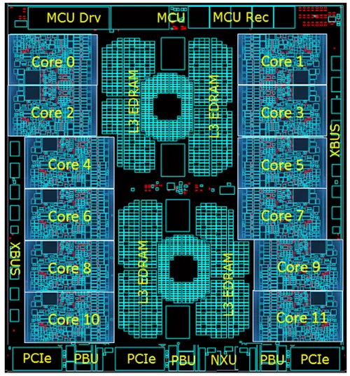
Central Processor (CP) Chip[edit]
- 14HP FinFET on SOI
- 17 metal layers
- 9,200,000,000 transistors
- 15.6 miles of wire
- 26,200,000,000 wire connections
- 5.2 GHz
- 12 cores
- Die size
- 25.3 mm x 27.5 mm
- 695.75 mm²
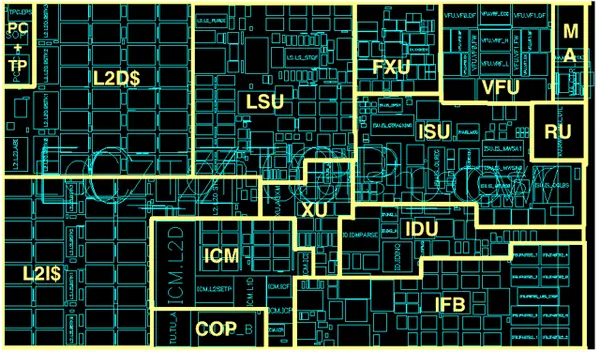
Core[edit]
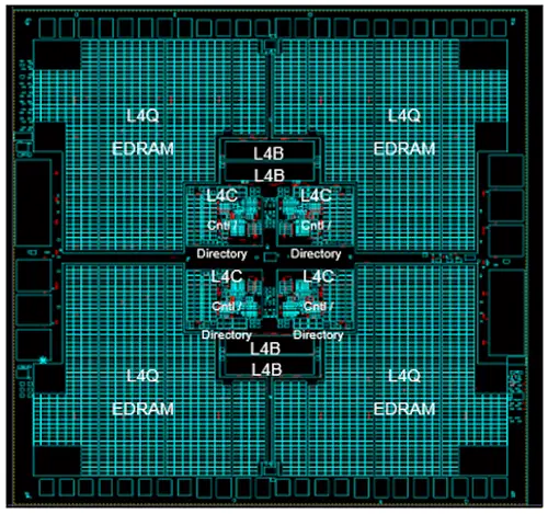
System Controller (SC) Chip[edit]
- 14HP FinFET on SOI
- 17 metal layers
- 12,200,000,000 transistors
- ~20,000 C4s
- 13.5 miles of signal wire
- 960 MiB shared eDRAM L4 cache.
- Die size
- 25.3 mm x 27.5 mm
- 695.75 mm²
| codename | z15 + |
| core count | 12 +, 9 +, 10 + and 11 + |
| designer | IBM + |
| first launched | September 12, 2019 + |
| full page name | ibm/microarchitectures/z15 + |
| instance of | microarchitecture + |
| instruction set architecture | z/Architecture + |
| manufacturer | GlobalFoundries + |
| microarchitecture type | CPU + |
| name | z15 + |
| pipeline stages | 17 + |
| process | 14 nm (0.014 μm, 1.4e-5 mm) + |
