| Edit Values | |
| Cortex-M55 µarch | |
| General Info | |
| Arch Type | CPU |
| Designer | ARM Holdings |
| Manufacturer | TSMC |
| Introduction | February 10, 2020 |
| Process | 55 nm, 45 nm, 32 nm, 28 nm, 22 nm, 16 nm, 10 nm, 7 nm, 5 nm |
| Core Configs | 1, 2, 4 |
| Pipeline | |
| Type | Scalar, Pipelined |
| OoOE | No |
| Speculative | No |
| Reg Renaming | No |
| Stages | 4-5 |
| Decode | 1-2-way |
| Instructions | |
| ISA | ARMv8.1-M |
| Extensions | FPU, Helium |
| Cache | |
| L1I Cache | 0-64 KiB/core 2-way set associative |
| L1D Cache | 0-64 KiB/core 4-way set associative |
| Succession | |
Cortex-M55 is an ultra-low-power ARM microarchitecture designed by ARM Holdings for microcontrollers and embedded subsystems. This microarchitecture is designed as a synthesizable IP core and is sold to other semiconductor companies to be implemented in their own chips. The Cortex-M55, which implements the ARMv8.1-M ISA, is an ultra-low-power core which is often found in microcontrollers, low-power chips, and in the embedded subsystems of more powerful chips.
Contents
History[edit]
The Cortex-M55 was officially launched on February 10, 2020. Support for custom instructions will be added in 2021.
Process Technology[edit]
The Cortex-M55 is designed to be fabricated on various different process nodes ranging from very mature nodes such as the 130 nm to leading-edge 7 nm and 5 nm nodes.
Compiler support[edit]
| Compiler | Arch-Specific | Arch-Favorable |
|---|---|---|
| Arm Compiler | -mcpu=cortex-m55 |
-mtune=cortex-m55
|
| GCC | -mcpu=cortex-m55 |
-mtune=cortex-m55
|
| LLVM | -march=cortex-m55 |
-mtune=cortex-m55
|
Architecture[edit]
Key changes from Cortex-M7/Cortex-M4[edit]
- ARMv8.1-M (from ARMv7-M)
- 64-bit internal bus (from 32-bit)
- Performance
- Pipeline
- Bus
- New integration
- New coprocessor interface support
- New custom instructions
- New Helium extension support
- TrustZone for ARMv8-M
This list is incomplete; you can help by expanding it.
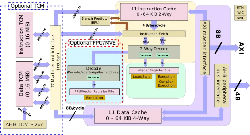
Block Diagram[edit]
Memory Hierarchy[edit]
The Cortex-M55 has a private L1I, L1D, I-TCM, and D-TCM. All four are configurable in size.
- Cache
- L1I Cache
- 0 - 64 KiB
- 2-way set associative
- Optional ECC support
- L1D Cache
- 0 - 64 KiB
- 4-way set associative
- Supports both write-back (WB) and write-through (WT)
- Optional ECC support
- L1I Cache
- TCM
- I-TCM
- 0 - 16 MiB
- Supports wait-states
- Optional ECC support
- D-TCM
- 0 - 16 MiB
- Supports wait-states
- Optional ECC support
- I-TCM
Overview[edit]
The Cortex-M55 is a synthesizable ultra-low-power core designed by Arm for an array of applications such as microcontrollers and embedded subsystems doing background work on more performant SoCs. Successionally and architecturally, the Cortex-M55 is the successor to the Cortex-M7 and the Cortex-M4, although in purely raw performance it's slightly behind the M7, though it makes up for it in new technologies such as its new vector extension. The Cortex-M55 is said to deliver 1.6 Dhrystone DMIPS/MHz and 4.2 CoreMark/MHz which is about 25% higher than the M4 but about 20% lower than the M7. In terms of frequency, the M55 is said to deliver up to 15% higher clock speed over the M4.
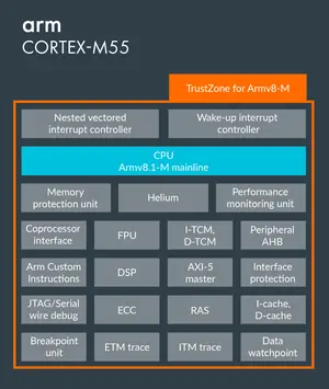
In addition to supporting the ARMv8.1-M ISA, the M55 introduces a number of upgrades and features, most of which are optional and configurable, including support for the coprocessor interface, Helium vector extension, and custom instructions. The architecture has additional optional support for MPUs, TrustZone, and tightly coupled memory (TCM).
Configuration[edit]
From a programming model (ISA) point of view, the Cortex-M55 supports five different major configurations. FPU can be included without Helium. Helium support for fixed-point vectored data types can be implemented without the FPU, while floating-point vector data types must include the FPU.
| Configuration | Base (Integer) | FPU (FP16, FP32, FP64) | Helium (Int8, Int16, Int 32) | Helium (FP16, FP32) |
|---|---|---|---|---|
| 1 | Included | - | - | - |
| 2 | Included | Included | - | - |
| 3 | Included | - | Included | - |
| 4 | Included | Included | Included | - |
| 5 | Included | Included | Included | Included |
Pipeline[edit]
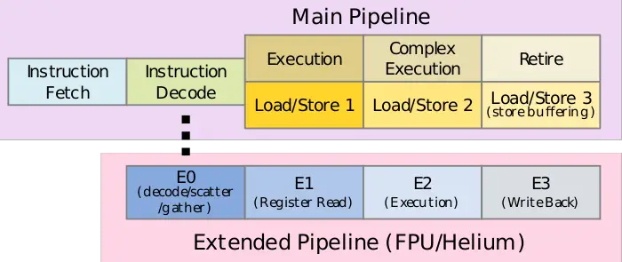
The Cortex-M55 is a 4-stage in-order scalar pipeline design. The design comprises of the main pipeline which is always present and an extended processing unit. The main pipeline is the typical integer pipeline designed to support the full ARMv8.1-M ISA. The extended processing unit is optional and is only present when the core implements the FPU or the Helium extensions. When the extended processing unit is present, that part of the pipeline is extended by an additional stage (for a total of 5 stages). The separate pipeline allows the core to go into retention state or be entirely power-down when not used.
Fetch & Decode[edit]
The M55 features a configurable private instruction cache. It is optional, but when present, it can be configured from 0 KiB to 64 KiB organized as a 2-way set associative. There is also optional ECC support if desired. Each cycle, four bytes are fetched from the instruction cache. There, instructions are pre-parsed and are sent to the decode. Since the ARMv8 supports a limited subset of T16, when two adjacent instructions are both 16-bit wide (T16+T16), the two instructions may be sent to decode to be decoded simultaneously. However, since the dual-issue capabilities are incredibly limited, Arm does not classify the design as a superscalar (unlike the capabilities of the Cortex-M7).
Execution[edit]
The M55 can do 1 64-bit load or store operation per cycle. Compared to the M7, the M55 can performance twice the MACs/cycle: 2x32-bit, 4x16-bit or 8x8-bit MACs/cycle.
Extended processing pipeline[edit]
From decode, the FPU and Helium instructions are routed to a separate pipeline. In order to save on power, that pipeline may go into a low-power retention state or be powered-down when not used. The extended processing pipeline is present if either the FPU or the Helium extensions are present. The FPU unit is based on the Arm FPv5 architecture. This is a fully IEEE-754 compliant FPU with support for half-precision, single-precision, and double-precision scalar floating-point data forms. Half-precision floating-point operations can be processed at twice the throughput per clock cycle as single-precision floats.
When the Helium extension is present, it reuses the FPU registers as vector registers, each being 128-bit wide. Internally, the vector unit is implemented with a 64-bit data path. This is twice as wide as prior Cortex-M designs but half the width of the ISA operations, therefore each operation takes two clock cycles to complete. The architecture permits overlapping execution cycles between instructions which are taken advantage of by the Cortex-M55, therefore when overlapping memory access and data processing operations together, both operations can be carried out in parallel.
Memory subsystem[edit]
The Cortex-M55 has a private data cache. It is optional and configurable from 0 KiB to 64 KiB in capacity organized as a 4-way set associative. The L1D$ supports both write-back and write-through policies as well as optional ECC support.
The Cortex-M55 features a fairly complex memory subsystem. The two main parts are the tightly-coupled memory (TCM) and the cache subsystem. Both are optional and both are configurable in sizes. The TCM is optimized for real-time applications with highly deterministic behaviors while the cache subsystem is designed for complex memory hierarchies, hiding higher latencies. The main bus interface to the Cortex-M55 from the rest of the system is the 64-bit AMBA 5 AXI. The interface supports multiple outstanding memory transfers as well as burst transfers and can operate at the core frequency or at some divided clock frequency.
There are a number of additional interfaces including a 32-bit AHB peripheral interface for legacy AHB peripherals. A debug AHB interface is a 32-bit debug AHB5 slave interface providing debug support for the Debug Access Port (DAP) to the memory system.
TCM subsystem[edit]
The TCM subsystem is somewhat similar to the one found in the Cortex-M7 but comes with a few noticeable differences. The TCM consists of an instruction TCM (I-TCM) and a data TCM (D-TCM). As with the M7, the purpose of the TCM subsystem is to provide deterministic latencies for real-time applications. The instruction TCM is optional and configurable from 0 to 16 MiB with optional ECC support. It is 32-bit wide, allowing up to 4 bytes per cycle to be transferred from the I-TCM to either the instruction fetch or the instruction memory. The D-TCM is also optional and is configurable from 0 to 16 MiB in capacity with optional ECC support. Whereas the Cortex-M7 featured two 32-bit data TCM interfaces, the M55 features four 32-bit data TCM interfaces which are split equally using address bits[3:2]. The data TCM interfaces collectively have an aggregated bandwidth of 128-bit per cycle, however since the Helium vector extension features an interface data path of 64-bit, software execution can only generate 64-bit data transfers per cycle. The rest of the bandwidth can be used for other purposes such as data memory access operations, transferring data from and to the TCM simultaneously while the data is read by the core execution. Accesses to TCM memory banks are prioritized for software execution, therefore an attempt by the DMA controller will be stalled while the software is reading from the same TCM bank.
All Cortex-M55 chips[edit]
| List of Cortex-M55-based Processors | ||||
|---|---|---|---|---|
| Model | Launched | Cores | Frequency | |
| Count: 0 | ||||
Bibliography[edit]
- Arm. personal communication. February 2020.
| codename | Cortex-M55 + |
| core count | 1 +, 2 + and 4 + |
| designer | ARM Holdings + |
| first launched | February 10, 2020 + |
| full page name | arm holdings/microarchitectures/cortex-m55 + |
| instance of | microarchitecture + |
| instruction set architecture | ARMv8.1-M + |
| manufacturer | TSMC + |
| microarchitecture type | CPU + |
| name | Cortex-M55 + |
| pipeline stages (max) | 5 + |
| pipeline stages (min) | 4 + |
| process | 55 nm (0.055 μm, 5.5e-5 mm) +, 45 nm (0.045 μm, 4.5e-5 mm) +, 32 nm (0.032 μm, 3.2e-5 mm) +, 28 nm (0.028 μm, 2.8e-5 mm) +, 22 nm (0.022 μm, 2.2e-5 mm) +, 16 nm (0.016 μm, 1.6e-5 mm) +, 10 nm (0.01 μm, 1.0e-5 mm) +, 7 nm (0.007 μm, 7.0e-6 mm) + and 5 nm (0.005 μm, 5.0e-6 mm) + |


