| Edit Values | |
| MLP µarch | |
| General Info | |
| Arch Type | NPU |
| Designer | Arm Holdings |
| Manufacturer | TSMC, Samsung, UMC |
| Introduction | 2018 |
| Process | 16 nm, 7 nm |
| PE Configs | 4, 8, 12, 16 |
Machine Learning Processor (MLP) is a first-generation neural processor microarchitecture designed by Arm for embedded and mobile SoCs as part of Project Trillium. This microarchitecture is designed as a synthesizable NPU IP and is sold to other semiconductor companies to be implemented in their own chips.
Contents
Process technology[edit]
Although the MLP is designed as a synthesizable IP, it has been specifically tuned for the 16 nanometer and 7 nanometer nodes.
Release date[edit]
Arm officially released the MLP under the Ethos family in late 2019.
Architecture[edit]
Block diagram[edit]
Full MLP[edit]
Compute Engine[edit]
Overview[edit]
The Machine Learning Processor (MLP) is Arm's first commercial neural processor microarchitecture as part of Project Trillium. The architecture itself was a ground-up design intended to provide significant performance-efficiency over the company's existing CPUs (Cortex) and GPUs (Mali) for neural network workloads with an emphasis and optimizations for CNNs and RNNs. In terms of power, the MLP is designed to scale from very low-power embedded IoT applications and up to complex mobile and network SoCs. Likewise, with performance, the architecture uses a configurable scalable design which, depending on the exact configuration, can span from 1 TOPS to as much as 10 TOPS.
The MLP microarchitecture is sold as synthesizable RTL IP with various SKUs under the Ethos family. Those SKUs come preconfigured with a fixed number of compute engines (CEs) and cache sizes designed to meet a certain performance level and power envelopes.
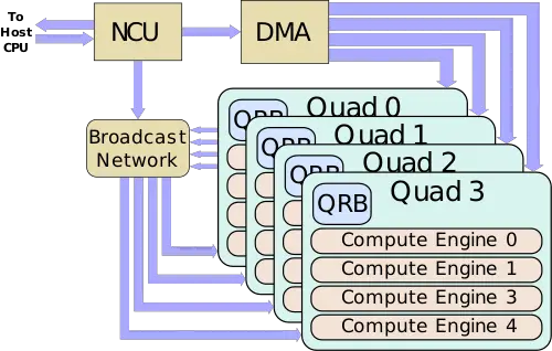
The MLP is fully statically scheduled by the compiler which takes a given neural network and maps it to a command stream. The toolchain also performs a number of additional optimizations ahead of time including compression (weights and feature maps are loaded into memory and into the MLP SRAM banks already compressed) and tiling. The command stream includes that necessary DMA operations such as the block fetching operations along with the accompanying compute operations. At a very high level, the MLP itself comprises a DMA engine, the network control unit (NCU), and a configurable number of compute engines (CEs). During runtime, the host processor loads the command stream onto the control unit which parses the stream and executes the operations by controlling the various functional blocks. The DMA engine is capable of talking to external memory while being aware of the various supported neural network layouts - allowing it to handle strides and other predictable NN memory operations, fetching the data for compute ahead of time. The compute engines are the workhorse component of the system. Each CE comprises two functional blocks, the MAC Compute Engine (MCE) and the Programmable Layer Engine (PLE). The MCE performs fixed-function multiply-accumulate operations efficiently on 8-bit integers while the PLE offers a more flexible programmable processor that supports vector operations and can implement more complex or less common operations. The architecture design relies on careful co-design with the compiler but yields more simplified hardware while enabling more deterministic performance characteristics.
Compute Engine (CE)[edit]
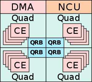
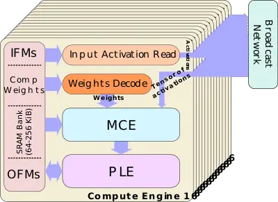
The MLP uses a scalable design that uses varying numbers of compute engines (CEs) which are grouped into Quads. A single MLP can come with as little as a single quad and with a single compute engine and all the way up to four quads and up to sixteen compute engines in a total. The compute engine is the main workhorse of the MLP. The three major components within the compute engine are the slice of SRAM, the MAC Compute Engine (MCE), and the Programmable Layer Engine (PLE). The difference MCE is designed for highly-efficient matrix multiply operations while the PLE is designed for flexibility by performing the various miscellaneous operations as well as providing additional functionality for implementing new and novel AI functions.
Convolutions optimizations[edit]
Each CE comes with a slice of SRAM. The exact size is identical for all the CEs in the MLP and are configurable in size from 64 KiB to 256 KiB. Since the entire execution is statically scheduled, at compile-time, the compiler will partition the SRAM into a number of sections including the input feature map (IFM) such as the input activations, the model weights in compressed form, and the output feature maps for the output activations.
During runtime, each compute engine is designed to work on a different output feature map, interleaved across the compute engines. The input feature map is interleaved across all the SRAM banks. The corresponding weights for each of the different output feature maps are residents in the SRAM of the CE which is processing it. During execution, each compute engine reads a 2D patch of the input feature map from its local SRAM and sends it to the Broadcast Network. The Broadcast Network unit takes those 2D patches and assembles a 3D block of input activations (a tensor) which is then broadcast to all MCEs in the MLP. While the broadcast goes on, the compressed weights from the local SRAM for a given output feature map are decompressed and sent to the MAC units as well. This allows all the MAC units in all the MCEs to work on the same block of input activations. The computed results for the output feature map are collected in 32b accumulators. The 32b values are then scaled down to 8b and are sent for additional post-processing by the PLE.
MAC Compute Engine (MCE)[edit]
The MAC Compute Engine (MCE) is designed for very efficient matrix multiply operations. The weights for each set of operations come from the weight decoder while the assembled tensor of activations comes from broadcast network. Arm has designed a POP IP version of the MCE which optimizes for the 16 nm and 7 nm nodes with a custom physical layout design.
Each MCE incorporates eight MAC units which are each capable of performing 16 8-bit dot product operations. In other words, each cycle up to 128 Int8 values may be multiplied by 128 additional Int8 values and be summed up into 32-bit accumulators. This puts the peak theoretical compute power of each MCE at 256 OPs/cycle. With up to 16 compute engines per MLP, the peak MLP compute is 4,096 OPS/cycle. With the MLP targetting frequencies of around 1 GHz, this translates to up to 4.1 TOPS. The real performance will vary depending on the utilization of the MCEs which depend on the parameters. The MCEs have some additional logic to optimize around sparsity, allowing datapath gating for zeros.
Note that although the MCEs are mainly designed for 8-bit operations, they can support 16-bit for things such as pixel sizes bigger than 8-bit. When operating in 16-bit, they run at 1/4th the throughput. In other words, they can do 64 (16-bit) OPs/cycle and up to 1024 OPs/cycle (1.024 TOPS at 1 GHz) for all 16 compute units.
At completion, the final 32b values are scaled back down to 8b values before they are sent to the PLE for further post-processing.
Programmable Layer Engine (PLE)[edit]
From the MCE, 8-bit results are fed into the PLE vector register file. The programmable layer engine (PLE) is designed for performing post-processing as well as flexibility for implementing custom functionalities. Once values arrive at the register file, the CPU kicks and operates the vector engine to perform the appropriate operations on the register file. The PLE features an Arm Cortex-M CPU with a 16-lane Vector Engine which supports the vector and neural network extensions, allowing it to do non-convolution operations more efficiently.
Following processing, the final results are DMA'ed back to the main SRAM bank. It's also worth noting that data need not only come from the MCE. For various operations, it's entirely possible for the PLE to fetch the data directly from the main SRAM bank to operate on certain data.
Die[edit]
- 7 nm process
- full 16 compute units configuration
- 1 MiB SRAM configuration
- ~4 TOPS @ 1 GHz
- > 3 TOPS/W
- 2.5 mm²
Bibliography[edit]
- Arm, IEEE Hot Chips 30 Symposium (HCS) 2018.
- Arm. personal communication. October, 2019.
- Arm. personal communication. February, 2020.
See also[edit]
| codename | MLP + |
| designer | Arm Holdings + |
| first launched | 2018 + |
| full page name | arm holdings/microarchitectures/mlp + |
| instance of | microarchitecture + |
| manufacturer | TSMC +, Samsung + and UMC + |
| name | MLP + |
| process | 16 nm (0.016 μm, 1.6e-5 mm) + and 7 nm (0.007 μm, 7.0e-6 mm) + |
| processing element count | 4 +, 8 +, 12 + and 16 + |


