Semiconductor & Computer Engineering
| Edit Values | |
| KiloCore | |
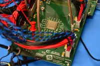 | |
| KiloCore on a daughterboard | |
| General Info | |
| Designer | UC Davis |
| Manufacturer | IBM |
| Introduction | June 17, 2016 (announced) |
| General Specs | |
| Frequency | 1,782 MHz |
| Microarchitecture | |
| Process | 32 nm |
| Transistors | 621,000,000 |
| Technology | CMOS |
| Die | 64 mm² |
| Word Size | 16 bit |
| Cores | 1,000 |
| Electrical | |
| Power dissipation | 39.6 W |
| Vcore | 1.1 V |

KiloCore is a prototype 16-bit MPPA chip containing 1,000 cores developed by the VLSI Computation Laboratory (VCL) at UC Davis. The chip, which was manufactured on IBM's 32 nm process PD-SOI technology, is said to have a maximum computation rate of 1.78 trillion instructions per second. This chip was presented at the 2016 Symposia on VLSI Technology and Circuits on June 17, 2016.
Contrary to many online reports, the KiloCore is not the world's first microprocessor to achieve 1,000 or more cores. A number of other processors, including the PEZY-SC, reached the milestone first.
Architecture
The chip is designed as a massively parallel processor array, with 992 cores arranged as a grid 32 by 31. 8 Additional cores are found along with 12 memory modules of 64 KB SRAM ea (for a total of 768 KB). Communication between cores is done via a circuit-switched network and a very-small-area packet router (see wormhole routing).
Cores
Each core is an independent processing unit capable of issuing one instruction in-order per cycle. Instructions may come from the local instruction memory or they may be fetched from one of the independent memory module. Likewise data may come from the data memory or from the independent memory module.
Each core contains 128x40-bit local instruction memory. Data memory is also stored in each as 2 banks of 128x16-bit each (for a total of 256x16-bit). The core also has three data address generators, two 32x16 input FIFO buffers, a 16-bit fixed-poit data path.
Memory Module
Each memory module contains 64 KB of SRAM and has an area of 0.164 mm². The module also contains two 32x16-bit FIFO buffers.
Floorplan

Each core has an area of 0.055 mm² (232 µm x 239 µm) and contains 575,000 transistors. The SRAM memory module has an area of 0.164 mm² (367 µm x 446 µm).
ISA
Each core supports 72 general instructions supporting signed and unsigned operations. The processor operates on 16-bit data word size with the exception of the multiply-accumulator which has a 40-bit output. Larger word size operations such as 32-bit may be emulated via software.
Cache
- Per core
- 640 bytes (128x40-bit) local instruction memory
- 512 bytes (256x16-bit) local data memory
- 768 KB SRAM on-die
- 12 shared SRAM memory modules, 64 KB each
Documents
- Aaron Stillmaker, "Design of Energy-Efficient Many-Core MIMD GALS Processor Arrays in the 1000-Processor Era," Ph.D Dissertation, Technical Report ECE-VCL-2015-1, VLSI Computation Laboratory, ECE Department, University of California, Davis, 2015.
- Brent Bohnenstiehl, Aaron Stillmaker, Jon Pimentel, Timothy Andreas, Bin Liu, Anh Tran, Emmanuel Adeagbo, Bevan Baas, "A 5.8 pJ/Op 115 Billion Ops/sec, to 1.78 Trillion Ops/sec 32nm 1000-Processor Array", VLSI Computation Laboratory, ECE Department, University of California, Davis, 2016.
| base frequency | 1,782 MHz (1.782 GHz, 1,782,000 kHz) + |
| core count | 1,000 + |
| core voltage | 1.1 V (11 dV, 110 cV, 1,100 mV) + |
| designer | UC Davis + |
| die area | 64 mm² (0.0992 in², 0.64 cm², 64,000,000 µm²) + |
| first announced | June 17, 2016 + |
| full page name | uc davis/kilocore + |
| instance of | microprocessor + |
| ldate | June 17, 2016 + |
| main image |  + + |
| main image caption | KiloCore on a daughterboard + |
| manufacturer | IBM + |
| name | KiloCore + |
| power dissipation | 39.6 W (39,600 mW, 0.0531 hp, 0.0396 kW) + |
| process | 32 nm (0.032 μm, 3.2e-5 mm) + |
| technology | CMOS + |
| transistor count | 621,000,000 + |
| word size | 16 bit (2 octets, 4 nibbles) + |