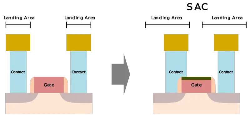
Self-Aligned Contact (SAC) is a semiconductor process flow technique that adds a protective dielectric layer over the transistor gate in order to prevent contact-to-gate shorts. SAC is used to enable aggressive scaling of the contacted poly pitch while minimizing yield loss due to misalignment and partial overlaps of the contacts over the gate.
Overview
On recent leading-edge nodes, the gate length no longer scales are much as they historically used to. Despite that slowdown, the contacted poly pitch continues to scale. The total working spaces include the area for the contacts, the gate length, and the two spacers. Unfortunately, since the gate length no longer scales as much as the CPP, the space length for the contacts is decreasing sharply. The trend is not sustainable and eventually, there was a need to be able to length much closer to the gate and even on top of the gate. In addition to the lack of space, problems with landing the contacts are exasperated by the tighter alignment tolerances and overlay issues due to multiple masks (e.g., SADP, SAQP).
The compounding issues have meant the industry needed to move to a self-aligned contact scheme. Under the self-aligned contact (SAC) flow, it's now possible to land the contacts much closer or even on top of the gate without creating a shot. This meant the contact poly pitch can continue to scale all while relaxing the alignment tolerances which means high die yield.
Bibliography
- Kaizad Mistry, Semicon 2012.
- Auth, Chris, et al. "A 22nm high performance and low-power CMOS technology featuring fully-depleted tri-gate transistors, self-aligned contacts and high density MIM capacitors." VLSI technology (VLSIT), 2012 symposium on. IEEE, 2012.

