(→Core cluster) |
(→Core) |
||
| Line 99: | Line 99: | ||
== Core == | == Core == | ||
| − | |||
=== Pipeline === | === Pipeline === | ||
The M1 has a speculatively executing [[out-of-order]] 4-wide pipeline. | The M1 has a speculatively executing [[out-of-order]] 4-wide pipeline. | ||
Revision as of 01:22, 4 February 2018
| Edit Values | |
| Mongoose 1 µarch | |
| General Info | |
| Arch Type | CPU |
| Designer | Samsung |
| Manufacturer | Samsung |
| Process | 14 nm |
| Pipeline | |
| OoOE | Yes |
| Speculative | Yes |
| Reg Renaming | Yes |
| Decode | 4-way |
| Instructions | |
| ISA | ARMv8 |
| Cache | |
| L1I Cache | 64 KiB/core 4-way set associative |
| L1D Cache | 32 KiB/core 8-way set associative |
| L2 Cache | 2 MiB/cluster 16-way set associative |
| Succession | |
Mongoose 1 (M1) is an ARM microarchitecture designed by Samsung for their consumer electronics. This was Samsung's first in-house developed high-performance low-power ARM microarchitecture.
Contents
History
The Mongoose 1 (M1) microarchitecture was Samsung's first in-house design which was done entirely from scratch. A design team was assembled and in roughly 3 years, they've gone from requirements to tape-out. The design was done at Samsung's Austin R&D Center (SARC) which was founded in 2010 for the sole purpose of developing high-performance, low-power, complex CPU and System IPs. A large portion of the design team consists of many ex-AMD Austin engineers as well as ex-IBMers.
Process Technology
M1 was fabricated on Samsung's 14 nm process.
Architecture
The M1 is Samsung's first in-house design from scratch.
- ARM v8.0
- 2.6 GHz clock frequency
- 2.3 GHz for multi-core workloads
- Sub 3-watt/core
- 14 nm process (FinFET)
- Core
- Advanced branch predictor
- 4-way instruction decode
- Most instructions map to a single µOP, with a few exceptions
- 4-way µOP dispatch and retire
- Out-of-order execution
- Out-of-order load and stores
- Multistride/multistream prefetcher
- Low-latency and low-power caches
Block Diagram
Core Cluster Overview
Individual Core
Memory Hierarchy
- Cache
- L1I Cache
- 64 KiB, 4-way set associative
- 128 B line size
- per core
- Parity-protected
- 64 KiB, 4-way set associative
- L1D Cache
- 32 KiB, 8-way set associative
- 64 B line size
- per core
- 4 cycles for fastest load-to-use
- 16 B/cycle load bandwidth
- 16 B/cycle store bandwidth
- 32 KiB, 8-way set associative
- L2 Cache
- 2 MiB, 16-way set associative
- 4x banks (512 KiB each)
- Inclusive of L1
- 22 cycles latency
- 16 B/cycle/CPU bandwidth
- 2 MiB, 16-way set associative
- L1I Cache
Mongoose 1 TLB consists of dedicated L1 TLB for instruction cache (ITLB) and another one for data cache (DTLB). Additionally there is a unified L2 TLB (STLB).
- TLBs
- ITLB
- 256-entry
- DTLB
- 32-entry
- STLB
- 1,024-entry
- Per core
- ITLB
- BPU
- 4K-entry main BTB
- 64-entry µBTB
- 64-entry return stack
Overview
Mongoose 1 was an entirely brand new architecture from the ground up that implemented the ARMv8 ISA. The architecture supports both AArch64 and AArch32 including Thumb modes. The architecture is a quad-core design which was intended to be paired with another low-power ARM IP core.
Core
Pipeline
The M1 has a speculatively executing out-of-order 4-wide pipeline.
Front-end
The front-end is responsible for fetching the correct stream of bytes from the cache based on the traffic flow predictions by the branch predictor and feeding the decoders which decode the instructions into simple signals. The goal of the front-end is the ultimately keep the back-end busy executing as much instructions as possible.
Fetch & pre-decoding
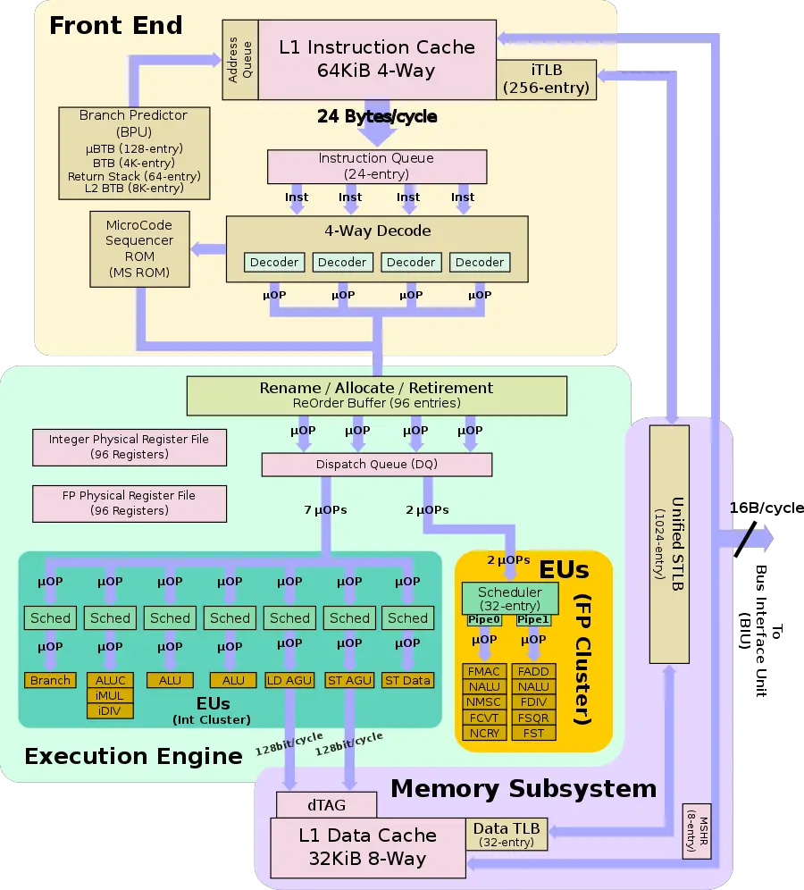
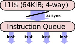
With the help of the branch predictor, the instructions should already be found in the level 1 instruction cache. The L1I cache is 64 KiB, 4-way set associative and has its own iTLB consisting of 256 entries. Up to 24 bytes are read from it each cycle into the instruction queue which allows them to hide very short branch bubbles. The instruction queue is a slightly more complex component than a simple buffer. The byte stream gets split up into the ARM instructions its made off, including dealing with the various mis-aligned ARM instructions such as in the case of thumb mode.
Decoding
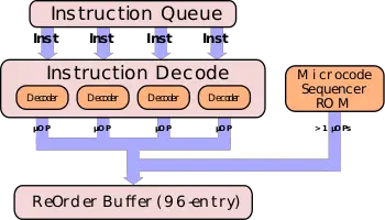
From the instruction queue the instructions are sent to decode. Decode is a 4-way decoder which can handle both the ARM AArch64 and AArch32 instructions. Up to four µOPs are decoded and sent to the re-order buffer.
Micro-Sequencer
For some complex ARM instructions such as the ARMv7 load-store multiples instructions which result in multiple µOPs being emitted, M1 has a side micro-sequencer that will get invoked and emit the appropriate µOPs.
Execution engine
Renaming & Allocation
As with the decode, up to four µOPs can be renamed each cycle. For some special cases such as in ARMv7 where four single-precision registers can alias into a single quad register or a pair of doubles, M1 has special logic in the rename area to handle the renaming of those floating point µOPs. For the case of a branch misprediction, M1 has a perform fast map recovery ability as a branch misprediction recovery mechanism.
M1 has a 96-entry reorder buffer which feeds the dispatch queue 4 µOPs per cycle.
Dispatch
From the dispatch queue, up to 7 µOPs may be issued to the integer cluster and up to 2 µOPs may be issued to the floating point cluster.
Integer cluster
The dispatch queue feeds the execution units. For integers, there is a 96-entry integer physical register file (roughly 35-36 of them is architected) which means data movement is not necessary. In the integer execution cluster, up to 7 µOPs per cycle may be dispatched to the schedulers. The schedulers are distributed across the various pipes. In total the integer schedulers have 58 entries and those entries are distributed in mixed sizes across the 7 schedulers.
For the first pipe the M1 has a branch resolution unit. The next three pipes have integer ALUs with only the first one capable of also multiplication and division. It's worth pointing out that while all three pipes are capable of execution the typical integer ALU µOPs (i.e., two source µOPs), only the first pipe (specifically marked as "ALUC") can also execute three source µOPs. This includes some of the ARMv7 special predicate forms.
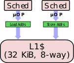
The last three pipes are for the load address adder, store address adder, and store data.
Floating-point cluster
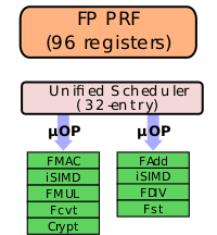
On the floating point cluster side, up to 2 µOPs may be issued to a unified scheduler which consists of 32 entries. There is a 96-entry floating point (vector) physical register file (roughly 35-36 architected). There are two pipes. The first one features a 5-cycle FMAC and a 4-cycle multiplier while the second pipe incorporates a 3-cycle floating-point adder. Additionally, the first pipe also includes a cryptography unit.
Retirement
Once execution is complete, µOPs may retire at a rate of up to 4 µOPs per cycle.
Memory subsystem
The M1 has a 32 KiB 8-way set associative level 1 data cache which is ECC protected. Loads and stores are done fully out of order with all the typical forwarding and light prediction that prevents thrashing. The M1 is capable of a single 128-bit load each cycle and a single 128-bit store each cycle. Note that both operations can be done at the same cycle. The level 1 data cache has a 4-cycle load latency and can support 8 outstanding misses to the L2 hierarchy.
The M1 has a multi-stride prefetcher which allows it to detect patterns and start the fetching request ahead of execution. While Samsung hasn't gone into too much detail, they noted that there is also some stream/copy optimizations as well which accelerate certain observable traffic patterns.
Core cluster
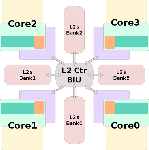
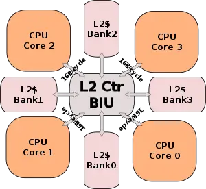
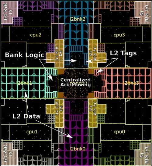
The M1 consists of four cores and a shared level 2 cache. Samsung has gone with a four-bank hierarchy with the L2. It is 2 MiB, 16-way set associative and ECC protected broken into 4 banks. Being inclusive of the L1, there are filtering being done for the L1 first. The bank storing the data depends on the address. The exact organization was not detailed. Each bank can return up to 16 bytes per cycle to the cores and has a 22-cycle latency.
Die
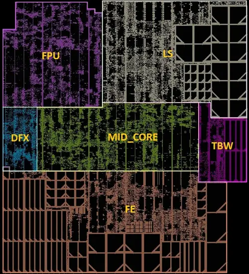
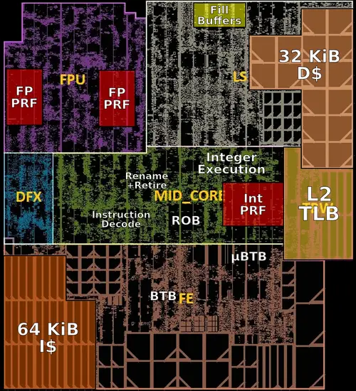
Core Floorplan
Core Cluster Floorplan
References
- Burgess, Brad. "Samsung exynos M1 processor." Hot Chips 28 Symposium (HCS), 2016 IEEE. IEEE, 2016.
| codename | Mongoose 1 + |
| designer | Samsung + |
| full page name | samsung/microarchitectures/m1 + |
| instance of | microarchitecture + |
| instruction set architecture | ARMv8 + |
| manufacturer | Samsung + |
| microarchitecture type | CPU + |
| name | Mongoose 1 + |
| process | 14 nm (0.014 μm, 1.4e-5 mm) + |
