From WikiChip
Difference between revisions of "intel/microarchitectures/gen9.5"
(→Models) |
|||
| Line 84: | Line 84: | ||
<references group=devID /> | <references group=devID /> | ||
| + | |||
| + | == Hardware Accelerated Video == | ||
| + | {{kaby lake hardware accelerated video table}} | ||
| + | |||
| + | == Process Technology == | ||
| + | {{main|intel/microarchitectures/kaby lake#Process_Technology|l1=Kaby Lake § Process Technology}} | ||
| + | Gen9 .5LP are part of the Kaby Lake SoC die which uses an enhanced [[14 nm process|14nm+ process]]. | ||
| + | |||
| + | == Architecture == | ||
| + | Gen9.5 LP is very similar to {{\\|Gen9 LP}} with a number of enhancements. | ||
| + | |||
| + | === Key changes from {{\\|Gen9 LP}} === | ||
| + | {{empty section}} | ||
| + | |||
| + | === Block Diagram === | ||
| + | ==== Entire SoC Overview ==== | ||
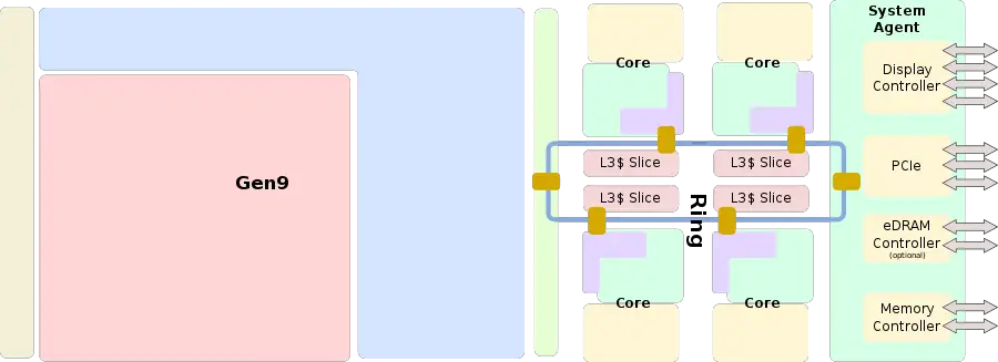
| + | [[File:skylake soc block diagram.svg|900px]] | ||
| + | ==== Gen9 LP ==== | ||
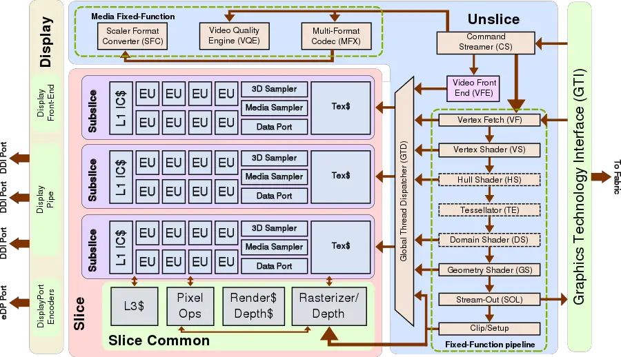
| + | This block is for the most common setup, which is GT2 with 24 execution units. | ||
| + | |||
| + | [[File:gen9 lp gt2 block diagram.svg|900px]] | ||
| + | ==== Individual Core ==== | ||
| + | See {{intel|Kaby Lake#Individual_Core|l=arch}}. | ||
Revision as of 15:09, 27 January 2017
| Edit Values | |
| Gen9.5 LP µarch | |
| General Info | |
| Arch Type | GPU |
| Designer | Intel |
| Manufacturer | Intel |
| Introduction | August 30, 2016 |
| Process | 14 nm |
| Succession | |
Gen9.5 LP (Generation 9.5 Low Power) is the microarchitecture for Intel's graphics processing unit utilized by Kaby Lake-based microprocessors. Gen9.5 LP is the successor to Gen9 LP used by Skylake and introduces a number of light enhancements.
Contents
Codenames
Various models support different Graphics Tiers (GT) which provides different levels of performance. Some models also support an additional eDRAM side cache.
| Code Name | Description |
|---|---|
| GT1 | Contains 1 slice with 12 execution units. |
| GT2 | Contains 1 slice with 24 execution units. |
| GT3 | Contains 2 slices with 48 execution units. |
| GT3e | Contains 2 slices with 48 execution units. Has an additional eDRAM side cache. |
| Halo (GT4e) | Contains 3 slices with 72 execution units. Has an additional eDRAM side cache. |
Models
| Gen9.5 LP IGP Models | Standards | ||||||||||||
|---|---|---|---|---|---|---|---|---|---|---|---|---|---|
| Name | Execution Units | Tier | Series | eDRAM | Vulkan | Direct3D | OpenGL | OpenCL | |||||
| Windows | Linux | Windows | Linux | HLSL | Windows | Linux | Windows | Linux | |||||
| HD Graphics 610 | 12 | GT1 | S, U | - | 1.0 | 12 | N/A | 5.1 | 4.4 | 4.5 | 2.0 | ||
| HD Graphics 615 | 24 | GT2 | Y | - | |||||||||
| HD Graphics 620 | 24 | GT2 | U | - | |||||||||
| HD Graphics 630 | 24 | GT2 | S, H | - | |||||||||
| HD Graphics P630 | 24 | GT2 | H | - | |||||||||
| Iris Plus Graphics 640 | 48 | GT3e | U | 64 MiB | |||||||||
| Iris Plus Graphics 650 | 48 | GT3e | U | 64 MiB | |||||||||
| Model | SKU | EUs | CPU Stepping[devID 1] | GT Stepping[devID 2] | Device2 ID[devID 3] | GT Device2 ID Revision[devID 4] |
|---|---|---|---|---|---|---|
| HD Graphics 610 | KBL DT 2+1F | 12 | 0x5902 | |||
| KBL U - ULT 2+1F | 0x5906 | |||||
| HD Graphics 615 | KBL Y - ULX 2+2 | 24 | 0x591E | |||
| HD Graphics 620 | KBL-U 2+2 | H0 | C0/B0 | 0x5916 | 0x2 | |
| HD Graphics 630 | KBL-S 4+2 | B0 | F0/C0 | 0x5912 | 0x4 | |
| KBL Halo 4+2 | 0x591B | |||||
| HD Graphics P630 | KBL WKS 4+2 | 0x591D | ||||
| Iris Plus Graphics 640 | KBL-U 2+3 | 48 | J1 | D1/B1 | 0x5926 | 0x6 |
| Iris Plus Graphics 650 | KBL U - ULT 2+3E (28W) | 0x5927 |
- ↑ The CPU Stepping is the actual CPU design stepping.
- ↑ The GT Stepping refers to the GT design stepping.
- ↑ The Device2 ID is the PCI device ID that identifies the GT SKU for driver software
- ↑ The GT Device2 Revision ID identifies the silicon stepping for driver software.
Hardware Accelerated Video
| [Edit] Kaby Lake (Gen9.5) Hardware Accelerated Video Capabilities | |||||||
|---|---|---|---|---|---|---|---|
| Codec | Encode | Decode | |||||
| Profiles | Levels | Max Resolution | Profiles | Levels | Max Resolution | ||
| MPEG-2 (H.262) | Main | High | 1080p (FHD) | Main | Main, High | 1080p (FHD) | |
| MPEG-4 AVC (H.264) | High, Main | 5.1 | 2160p (4K) | Main, High, MVC, Stereo | 5.1 | 2160p (4K) | |
| JPEG/MJPEG | Baseline | - | 16k x 16k | Baseline | Unified | 16k x 16k | |
| HEVC (H.265) | Main, Main 10 | 5.1 | 2160p (4K) | Main, Main 10 | 5.1 | 2160p (4K) | |
| VC-1 | ✘ | Advanced, Main, Simple | 3, High, Simple | 3840x3840 | |||
| VP8 | Unified | Unified | N/A | 0 | Unified | 1080p | |
| VP9 | 0 | 2160p (4K) | 0, 2 | Unified | 2160p (4K) | ||
Process Technology
- Main article: Kaby Lake § Process Technology
Gen9 .5LP are part of the Kaby Lake SoC die which uses an enhanced 14nm+ process.
Architecture
Gen9.5 LP is very similar to Gen9 LP with a number of enhancements.
Key changes from Gen9 LP
| This section is empty; you can help add the missing info by editing this page. |
Block Diagram
Entire SoC Overview
Gen9 LP
This block is for the most common setup, which is GT2 with 24 execution units.
Individual Core
Facts about "Gen9.5 - Microarchitectures - Intel"
| codename | Gen9.5 LP + |
| designer | Intel + |
| first launched | August 30, 2016 + |
| full page name | intel/microarchitectures/gen9.5 + |
| instance of | microarchitecture + |
| manufacturer | Intel + |
| microarchitecture type | GPU + |
| name | Gen9.5 LP + |
| process | 14 nm (0.014 μm, 1.4e-5 mm) + |


