From WikiChip
TSARLET - Microarchitectures - CEA Leti
| Edit Values | |
| TSARLET µarch | |
| General Info | |
| Arch Type | CPU |
| Designer | CEA-Leti |
| Manufacturer | STMicroelectronics |
| Process | 28 nm, 65 nm |
| Core Configs | 96 |
| Pipeline | |
| Type | Scalar, Single-issue |
| OoOE | No |
| Speculative | No |
| Reg Renaming | No |
| Stages | 5 |
| Decode | 1-way |
| Instructions | |
| ISA | MIPS32v1 |
| Cache | |
| L1I Cache | 16 KiB/core |
| L1D Cache | 16 KiB/core |
| L2 Cache | 256 KiB/core |
| L3 Cache | 1 MiB/core |
TSARLET was a research microarchitecture designed by CEA-Leti demonstarting the theoretical capabilities of a large-scale high-performance 3D stacked chiplets-based SoC technology. The project comprised 96 MIPS cores built using 6 chiplets 3D stack on an active interposer in order to demonstarte in-package silicon scale-out capabilities with superior inter-chip capabilities while reducing the overall power and production cost.
Contents
Architecture
Memory Hierarchy
| This section is empty; you can help add the missing info by editing this page. |
Overview
| This section is empty; you can help add the missing info by editing this page. |
Die
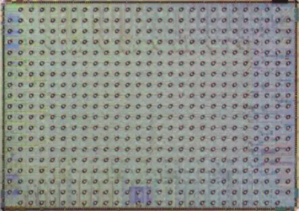
Compute chiplet
- STMicroelectronics 28 nm FDSOI
- 10 metal layers
- 4 mm x 5.6 mm (22 mm²) silicon area
- 395,000,000 transistors
- I/O
- 2D
- 249 signal, 237 power
- C4 bumps, 200 µm pitch
- 3D
- 2618 signal
- up to metal 10 @ 20 µm pitch
- 2D
Base interposer die
Facts about "TSARLET - Microarchitectures - CEA Leti"
| codename | TSARLET + |
| core count | 96 + |
| designer | CEA-Leti + |
| full page name | cea-leti/microarchitectures/tsarlet + |
| instance of | microarchitecture + |
| instruction set architecture | MIPS32v1 + |
| manufacturer | STMicroelectronics + |
| microarchitecture type | CPU + |
| name | TSARLET + |
| pipeline stages | 5 + |
| process | 28 nm (0.028 μm, 2.8e-5 mm) + and 65 nm (0.065 μm, 6.5e-5 mm) + |
