From WikiChip
ARMADA 610 - Marvell
| Edit Values | |
| ARMADA 610 | |
| General Info | |
| Designer | Marvell |
| Manufacturer | TSMC |
| Model Number | 610 |
| Part Number | 88AP610 |
| Market | Mobile |
| Introduction | October 19, 2009 (announced) January 5, 2010 (launched) |
| General Specs | |
| Family | ARMADA 600 |
| Series | 600 |
| Frequency | 1,000 MHz |
| Microarchitecture | |
| ISA | ARMv6 (ARM), ARMv5 |
| Microarchitecture | Sheeva PJ4 |
| Platform | ARMADA |
| Core Name | Sheeva PJ4 |
| Process | 55 nm |
| Word Size | 32 bit |
| Cores | 1 |
| Threads | 1 |
| Max Memory | 2 GiB |
| Multiprocessing | |
| Max SMP | 1-Way (Uniprocessor) |
| Electrical | |
| VI/O | 1.5 V ± 0.3 V, 3.0 V, 3.3 V |
ARMADA 610 was a 32-bit ARM microprocessor introduced by Marvell in 2010. This processor, which is based on Marvell's Sheeva PJ4 microarchitecture, operated at 1 GHz and supported up to 2 GiB of DDR3-1066 memory. The ARMADA 610 also integrated a Vivante GC860 IGP as well as an EPD display controller which eliminates page turn lag.
Contents
Cache
- Main article: Sheeva PJ4 § Cache
|
Cache Organization
Cache is a hardware component containing a relatively small and extremely fast memory designed to speed up the performance of a CPU by preparing ahead of time the data it needs to read from a relatively slower medium such as main memory. The organization and amount of cache can have a large impact on the performance, power consumption, die size, and consequently cost of the IC. Cache is specified by its size, number of sets, associativity, block size, sub-block size, and fetch and write-back policies. Note: All units are in kibibytes and mebibytes. |
|||||||||||||||||||||||||
|
|||||||||||||||||||||||||
Memory controller
|
Integrated Memory Controller
|
||||||||||||||
|
||||||||||||||
Static Memory Controller
- 4 chip selects, up to 256 MB each
- Asynch/Sync operation up to 78 MHz
- A/D and AA/D Mode, x8 & x16 NOR Flash interface
- Support for VLIO or companion chips
NAND Flash Controller
- ONFI compliant controller supporting SLC and MLC NAND, x8 & x16, small block and large block
- 2 Chip Selects with up to 64GB of address space
- Support for 2 KB and 4 KB page sizes
- 2-bit detect/1-bit correct ECC & 16-bit correct BCH
MMC, SD and SDIO Controller
- 4x MMC/SD/SDIO/CE-ATA Controllers
- Supports MMC/eMMC v4.2, 4.3 and 4.4
- SDIO v 2.0, SDcard v2.1 and v3.0 (UHS-I)
- CE-ATA 1/4/8-Bit, SPI mode and boot suppor
Expansions
|
Expansion Options
|
||||||||||||||||||
|
||||||||||||||||||
Graphics
The 618 incorporates a Vivante GC860 GPU capable of 45 million triangle strips per second, 250 Mpixel/s fill rate.
|
Integrated Graphics Information
|
||||||||||||||||||||||||||||||||||||||||
|
||||||||||||||||||||||||||||||||||||||||
- 1080p decode support for H.264 high profile, VC-1/WMV, MPEG-4, MPEG-2, H.263, On-2.
- 1080p encode support for h.264 high profile, MPEG-4, MPEG-2, H.263 and On-2.
Hardware Accelerators
Marvell Wireless Trusted Module v3
- Hashing units: MD5, SHA-1, HMAC-SHA-1; SHA-224/SHA256 and HMAC, SHA-512 and HMAC, MD5 and HMAC-MD5
- Symmetric crypto: AES (128 to 256 & ECB, CBC, CTR/XTS modes), DES/3DES (ECB & CBC), RC4
- Asymmetric crypto: ECC (Prime field ECC, FIPS std curve EC-224/256, EC-DSA) & RSA (RSA key gen, PKCS#1 v1.5/v2.1 Digital Signatures, x.509 Digital Certificate), & DiffieHellman Key exchange. True HW RNG, FIPS 140-2 certification
Features
[Edit/Modify Supported Features]
|
Supported ARM Extensions & Processor Features
|
||||||
|
||||||
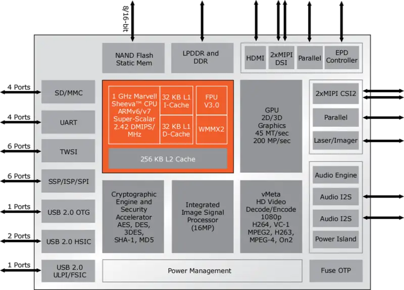
Block Diagram
Documents
Facts about "ARMADA 610 - Marvell"
| base frequency | 1,000 MHz (1 GHz, 1,000,000 kHz) + |
| core count | 1 + |
| core name | Sheeva PJ4 + |
| designer | Marvell + |
| family | ARMADA 600 + |
| first announced | October 19, 2009 + |
| first launched | January 5, 2010 + |
| full page name | marvell/armada/610 + |
| has ecc memory support | false + |
| instance of | microprocessor + |
| integrated gpu | GC860 + |
| integrated gpu designer | Vivante + |
| io voltage | 1.5 V (15 dV, 150 cV, 1,500 mV) +, 3 V (30 dV, 300 cV, 3,000 mV) + and 3.3 V (33 dV, 330 cV, 3,300 mV) + |
| io voltage tolerance | 0.3 V + |
| isa | ARMv5 + and ARMv6 + |
| isa family | ARM + |
| l1$ size | 64 KiB (65,536 B, 0.0625 MiB) + |
| l1d$ size | 32 KiB (32,768 B, 0.0313 MiB) + |
| l1i$ size | 32 KiB (32,768 B, 0.0313 MiB) + |
| l2$ size | 0.25 MiB (256 KiB, 262,144 B, 2.441406e-4 GiB) + |
| ldate | January 5, 2010 + |
| manufacturer | TSMC + |
| market segment | Mobile + |
| max cpu count | 1 + |
| max memory | 2,048 MiB (2,097,152 KiB, 2,147,483,648 B, 2 GiB, 0.00195 TiB) + |
| max memory bandwidth | 7.942 GiB/s (8,132.608 MiB/s, 8.528 GB/s, 8,527.658 MB/s, 0.00776 TiB/s, 0.00853 TB/s) + |
| max memory channels | 1 + |
| microarchitecture | Sheeva PJ4 + |
| model number | 610 + |
| name | ARMADA 610 + |
| part number | 88AP610 + |
| platform | ARMADA + |
| process | 55 nm (0.055 μm, 5.5e-5 mm) + |
| series | 600 + |
| smp max ways | 1 + |
| supported memory type | DDR2-800 + and DDR3-1066 + |
| thread count | 1 + |
| word size | 32 bit (4 octets, 8 nibbles) + |
