From WikiChip
Socket FM1 - AMD
| Edit Values | |
| Socket FM1 | |
| General Info | |
| Designer | AMD |
| Introduction | June 30, 2011 (launched) |
| Market | Desktop |
| Microarchitecture | K10 |
| TDP | 100 W 100,000 mW 0.134 hp 0.1 kW |
| Package | |
| Name | OPGA-905 |
| Type | Organic Micro Pin Grid Array |
| Contacts | 905 |
| Dimension | 40.0 mm 4 cm × 40.0 mm1.575 in 4 cm 1.575 in |
| Pitch | 1.27 mm 0.05 in |
| Socket | |
| Name | Socket FM1 |
| Type | PGA |
Socket FM1 was the socket for OPGA-905-packaged AMD microprocessors, the first generation of AMD APUs, desktop processors with integrated graphics. Its counterpart for mobile processors is Socket FS1. Socket FM1 was superseded by Socket FM2.
All processors for Socket FM1, codename "Llano", are members of AMD's Family 12h with CPU cores based on the K10 microarchitecture, and were fabricated on a 32 nm SOI process.
Contents
Features
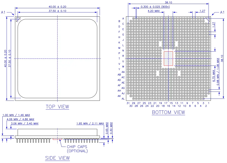
- 905-pin lidded micro pin grid array package, 1.27 mm pitch, 31 × 31 pins, 40 × 40 mm, organic substrate
- 2 × 64/72 bit DDR3 SDRAM interface up to 933 MHz, PC3-14900 (DDR3-1866), 29.9 GB/s
- Up to 4 UDIMMs or SODIMMs (2 per channel), up to 16 Gbyte per UDIMM, ECC supported
- JEDEC 1.5V, 1.35V
- PCIe Gen 1.0 and 2.0 (5 GT/s)
- Configurable x16 external graphics card (GFX) link (x16, x8, x4, up to 2 ports, DDI)
- Configurable x4 General Purpose Ports (1x4, 2x2, 1x2 + 2x1, 4x1)
- x4 Unified Media Interface to FCH
- Two independent display controllers
- Six Digital Display Interfaces
- 2 × single link
- 4 × multiplexed with 1x4 (dual link DVI 1x8) GFX lanes each
- DisplayPort / eDP 1.1a
- Single/dual link DVI, HDMI 1.4a, HDCP
- Six Digital Display Interfaces
- Power Management
- AMD PowerNow! technology
- ACPI P-states, processor power states C0, C1, sleep states S0, S3, S4, S5
- Northbridge P-states
- PCIe core power gating, power-down for unused lanes
- Thermal Controls
- Sideband temperature control
- Hardware thermal control (HTC)
- Local HTC
- DRAM thermal protection
Chipsets
- AMD FCH A55/A75 "Hudson-D2/D3"
Processors using Socket FM1
- AMD A-Series APU
- AMD E2-Series APU
- AMD Athlon II X2, X4
- AMD Sempron X2
| List of all Socket FM1-based Processors | |||||||||||||||||||
|---|---|---|---|---|---|---|---|---|---|---|---|---|---|---|---|---|---|---|---|
| Model | Price | Process | Launched | µarch | Family | Core | C | T | Freq | Turbo | TDP | ||||||||
| Count: 0 | |||||||||||||||||||
Package Diagram
OPGA-905 package (UOF 905). All dimensions in millimeters.
Socket Outline
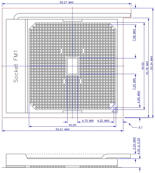
Socket FM1. All dimensions in millimeters.
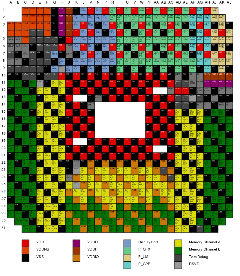
Pin Map
Pin Description
| Signal | Description |
|---|---|
| ALERT_L | Programmable pin that can indicate different events, including a SB-TSI interrupt |
| CLKIN_H/L | Differential PLL Reference Clock |
| DBREQ_L, DBRDY | Debug Request/Ready |
| DISP_CLKIN_H/L | Display Controller Reference Clock |
| DMAACTIVE_L | Indicates System DMA Activity to prevent NB P-state transition |
| DP0/DP1/DP2/DP3/DP4/DP5_AUXP/N | DisplayPort Auxiliary Channel |
| DP0/DP1/DP2/DP3/DP4/DP5_HPD | DisplayPort Hot Plug Detect |
| DP0/DP1_TXP/N[3:0] | DisplayPort Differential Transmitter |
| DP_AUX_ZVSS | Compensation Resistor to VSS |
| DP_BLON | Display Panel Backlight Enable |
| DP_DIGON | Display Panel Power Enable |
| DP_VARY_BL | Display Backlight Brightness Control |
| FM1R1 | |
| MA0/MA1/MB0/MB1_CS_L[1:0] | DRAM Chip Select |
| MA0/MA1/MB0/MB1_ODT[1:0] | DRAM Enable Pin for On Die Termination |
| MA/MB_ADD[15:0] | DRAM Column/Row Address |
| MA/MB_BANK[2:0] | DRAM Bank Address |
| MA/MB_CAS_L | DRAM Column Address Strobe |
| MA/MB_CHECK[7:0] | DRAM ECC Bits |
| MA/MB_CKE[1:0] | DRAM Clock Enable |
| MA/MB_CLK_H/L[7:0] | DRAM Differential Clock |
| MA/MB_DATA[63:0] | DRAM Data Bus |
| MA/MB_DM[8:0] | DRAM Data Mask |
| MA/MB_DQS_H/L[8:0] | DRAM Differential Data Strobe |
| MA/MB_EVENT_L | DRAM Thermal Event Status |
| MA/MB_RAS_L | DRAM Row Address Strobe |
| MA/MB_RESET_L | DRAM Reset Pin for Suspend-to-RAM Power Management Mode |
| MA/MB_WE_L | DRAM Write Enable |
| M_VREF | DRAM Interface Voltage Reference |
| M_ZVDDIO | Compensation Resistor to VDDIO |
| PROCHOT_L | Processor in HTC-active state |
| PWROK | Voltages and CLKIN have reached specified operation |
| P_GFX_TX/RXP/N[15:0] | External graphics card Transmit/Receive Data Differential Pairs |
| P_GPP_TX/RXP/N[3:0] | General Purpose Ports Transmit/Receive Data Differential Pairs |
| P_UMI_TX/RXP/N[3:0] | Unified Media Interface Transmit/Receive Data Differential Pairs |
| P_ZVDDP | Compensation Resistor to VDDP Power Supply |
| P_ZVSS | Compensation Resistor to VSS |
| RESET_L | Processor Reset |
| RSVD | Reserved |
| SIC, SID | Sideband Temperature Sensor Interface Clock/Data |
| SVC, SVD | Serial VID Interface Clock/Data |
| TCK, TDI, TDO, TMS, TRST_L | JTAG Interface |
| TEST* | Test signal |
| THERMDA, THERMDC | Thermal Diode Anode, Cathode |
| THERMTRIP_L | Thermal Sensor Trip output |
| VDD | Core Power Supply |
| VDD_SENSE | VDD Voltage Monitor Pin |
| VDDA | Filtered PLL Supply Voltage |
| VDDIO | DRAM I/O Ring Power Supply |
| VDDIO_SENSE | VDDIO Voltage Monitor Pin |
| VDDNB | Northbridge Power Supply |
| VDDNB_CAP_1 | |
| VDDNB_CAP_2 | |
| VDDNB_SENSE | VDDIO Voltage Monitor Pin |
| VDDP_A/B | |
| VDDP_SENSE | VDDP Voltage Monitor Pin |
| VDDR | VDDR Power Supply |
| VDDR_SENSE | VDDR Voltage Monitor Pin |
| VSS | Ground |
| VSS_SENSE | VSS Voltage Monitor Pin |
References
- "Socket FM1 Design Specification", AMD Publ. #47610, Rev. 3.00, August 2011
- "BIOS and Kernel Developer’s Guide (BKDG) For AMD Family 12h Processors", AMD Publ. #41131, Rev. 3.02, October 6, 2011
- "Family 12h AMD A-Series Accelerated Processor Product Data Sheet", AMD Publ. #49894, Rev. 3.01, October 2011
- "Family 12h AMD E2-Series Accelerated Processor Product Data Sheet", AMD Publ. #49895, Rev. 3.01, October 2011
- "Family 12h AMD Athlon™ II Processor Product Data Sheet", AMD Publ. #50322, Rev. 3.00, December 2011
- "Family 12h AMD Sempron™ Processor Product Data Sheet", AMD Publ. #50321, Rev. 3.00, December 2011
- "Revision Guide for AMD Family 12h Processors", AMD Publ. #44739, Rev. 3.10, March 21, 2012
See also
Facts about "Socket FM1 - AMD"
| designer | AMD + |
| first launched | June 30, 2011 + |
| instance of | package + |
| market segment | Desktop + |
| microarchitecture | K10 + |
| name | Socket FM1 + |
| package | OPGA-905 + |
| package contacts | 905 + |
| package length | 40 mm (4 cm, 1.575 in) + |
| package pitch | 1.27 mm (0.05 in) + |
| package type | Organic Micro Pin Grid Array + |
| package width | 40 mm (4 cm, 1.575 in) + |
| socket | Socket FM1 + |
| tdp | 100 W (100,000 mW, 0.134 hp, 0.1 kW) + |


