From WikiChip
Cloud AI 100 - Microarchitectures - Qualcomm
| Edit Values | |
| Cloud AI 100 µarch | |
| General Info | |
| Arch Type | NPU |
| Designer | Qualcomm |
| Manufacturer | TSMC |
| Introduction | March, 2021 |
| Process | 7 nm |
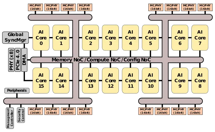
| PE Configs | 16 |
| Pipeline | |
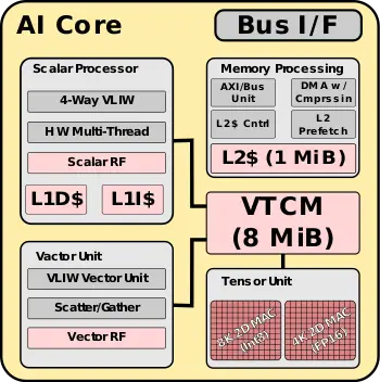
| Type | VLIW |
| Decode | 4-way |
| Cache | |
| L2 Cache | 1 MiB/core |
| Side Cache | 8 MiB/core |
Cloud AI 100 is an NPU microarchitecture designed by Qualcomm for the server and edge market. Those NPUs are sold under the Cloud AI brand.
Contents
Process Technology[edit]
The Cloud AI 100 SoC is fabricated on TSMC's 7-nanometer process.
Architecture[edit]
Key Features[edit]
Block Diagram[edit]
SoC[edit]
AI Core[edit]
Memory Hierarchy[edit]
- L1D$ / L1I$
- Private per AI Core
- L2
- 1 MiB / AI Core
- Vector Tightly-Coupled Memory (VTCM)
- 8 MiB / AI Core
- DRAM
- 8-32 GiB
- LPDDR4x-4266
- 68.25 - 136.5 GB/s
- LPDDR4x-4266
- 8-32 GiB
Overview[edit]
AI Core[edit]
Performance claims[edit]
Performance-per-watt was published by Quall based on an Int8 3×3 convolution operation with uniformly distributed weights and input action comprising 50% zeros which Qualcomm says is typical for Deep CNN with Relu operators. To that end, Qualcomm says the AI 100 can achieve up to ~150 TOPs at ~12 W at over 12 TOPS/W in edge cases and ~363 TOPs at under 70 W at 5.24 TOPs/W in data center uses. Numbers are at the SoC level.
| SoC Power | 12.05 W | 19.74 W | 69.26 W |
|---|---|---|---|
| TOPS | 149.01 | 196.94 | 363.02 |
| TOPS/W | 12.37 | 9.98 | 5.24 |
Bibliography[edit]
- Linley Fall Processor Conference 2021
- Qualcomm, IEEE Hot Chips 33 Symposium (HCS) 2021.
Facts about "Cloud AI 100 - Microarchitectures - Qualcomm"
| codename | Cloud AI 100 + |
| designer | Qualcomm + |
| first launched | March 2021 + |
| full page name | qualcomm/microarchitectures/cloud ai 100 + |
| instance of | microarchitecture + |
| manufacturer | TSMC + |
| name | Cloud AI 100 + |
| process | 7 nm (0.007 μm, 7.0e-6 mm) + |
| processing element count | 16 + |

