From WikiChip
Cloud AI 100 - Microarchitectures - Qualcomm
| Edit Values | |
| Cloud AI 100 µarch | |
| General Info | |
| Arch Type | NPU |
| Designer | Qualcomm |
| Manufacturer | TSMC |
| Introduction | March, 2021 |
| Process | 7 nm |
| PE Configs | 16 |
| Pipeline | |
| Type | VLIW |
| Decode | 4-way |
| Cache | |
| L2 Cache | 1 MiB/core |
| Side Cache | 8 MiB/core |
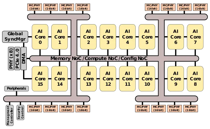
Cloud AI 100 is an NPU microarchitecture designed by Qualcomm for the server and edge market. Those NPUs are sold under the Cloud AI brand.
Contents
Process Technology
The Cloud AI 100 SoC is fabricated on TSMC's 7-nanometer process.
Architecture
Key Features
Block Diagram
SoC
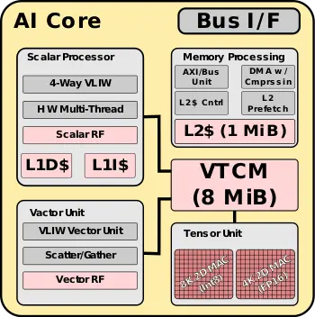
AI Core
Memory Hierarchy
- L1D$ / L1I$
- Private per AI Core
- L2
- 1 MiB / AI Core
- Vector Tightly-Coupled Memory (VTCM)
- 8 MiB / AI Core
- DRAM
- 8-32 GiB
- LPDDR4x-4266
- 68.25 - 136.5 GB/s
- LPDDR4x-4266
- 8-32 GiB
Overview
AI Core
Performance claims
Performance-per-watt was published by Quall based on an Int8 3×3 convolution operation with uniformly distributed weights and input action comprising 50% zeros which Qualcomm says is typical for Deep CNN with Relu operators. To that end, Qualcomm says the AI 100 can achieve up to ~150 TOPs at ~12 W at over 12 TOPS/W in edge cases and ~363 TOPs at under 70 W at 5.24 TOPs/W in data center uses. Numbers are at the SoC level.
| SoC Power | 12.05 W | 19.74 W | 69.26 W |
|---|---|---|---|
| TOPS | 149.01 | 196.94 | 363.02 |
| TOPS/W | 12.37 | 9.98 | 5.24 |
Bibliography
- Linley Fall Processor Conference 2021
- Qualcomm, IEEE Hot Chips 33 Symposium (HCS) 2021.
Facts about "Cloud AI 100 - Microarchitectures - Qualcomm"
| codename | Cloud AI 100 + |
| designer | Qualcomm + |
| first launched | March 2021 + |
| full page name | qualcomm/microarchitectures/cloud ai 100 + |
| instance of | microarchitecture + |
| manufacturer | TSMC + |
| name | Cloud AI 100 + |
| process | 7 nm (0.007 μm, 7.0e-6 mm) + |
| processing element count | 16 + |

