From WikiChip
Exynos M5 - Microarchitectures - Samsung
| Edit Values | |
| Lion M5 µarch | |
| General Info | |
| Arch Type | CPU |
| Designer | Samsung |
| Manufacturer | Samsung |
| Introduction | 2020 |
| Process | 7 nm |
| Core Configs | 2 |
| Pipeline | |
| Type | Superscalar, Superpipeline |
| OoOE | Yes |
| Speculative | Yes |
| Reg Renaming | Yes |
| Stages | 16 |
| Decode | 6-way |
| Instructions | |
| ISA | ARMv8.2 |
| Cache | |
| L1I Cache | 64 KiB/core 4-way set associative |
| L1D Cache | 64 KiB/core 8-way set associative |
| L2 Cache | 512 KiB/core 8-way set associative |
| L3 Cache | 2 MiB/cluster 16-way set associative |
| Succession | |
Exynos Mongoose 5 (M5) is the successor to the Mongoose 4, a 7 nm ARM microarchitecture designed by Samsung for their consumer electronics.
Contents
Process Technology
The M5 is fabricated on Samsung's 7 nm process (7LPP).
Compiler support
| Compiler | Arch-Specific | Arch-Favorable |
|---|---|---|
| GCC | -mcpu=exynos-m5 |
-mtune=exynos-m5
|
| LLVM | -mcpu=exynos-m5 |
-mtune=exynos-m5
|
Architecture
Key changes from M4
- Front end
- Larger instruction queue (60 entries, up from 48)
- Improved mispredict penalty (15 cycles, down from 16)
- Back end
- LSU execution units reorganized
- Two new 32b integer ALU pipes
- Floating-point execution units reorganized
- Three new dedicted NEON dot product EUs
- LSU execution units reorganized
This list is incomplete; you can help by expanding it.
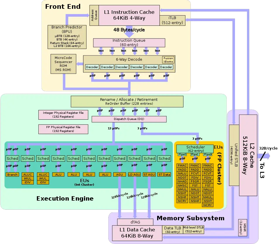
Block Diagram
Individual Core
Memory Hierarchy
- Cache
- L1I Caches
- 64 KiB, 4-way set associative
- 128 B line size
- per core
- Parity-protected
- 64 KiB, 4-way set associative
- L1D Cache
- 64 KiB, 8-way set associative
- 64 B line size
- per core
- 4 cycles for fastest load-to-use
- 32 B/cycle load bandwidth
- 16 B/cycle store bandwidth
- 64 KiB, 8-way set associative
- L2 Cache
- 512 KiB, 8-way set associative
- Inclusive of L1
- 12 cycles latency
- 32 B/cycle bandwidth
- L3 Cache
- 2 MiB, 16-way set associative
- 1 MiB slice/core
- Exlusive of L2
- ~37-cycle typical (NUCA)
- 2 MiB, 16-way set associative
- BIU
- 80 outstanding transactions
- L1I Caches
The M3 TLB consists of dedicated L1 TLB for instruction cache (ITLB) and another one for data cache (DTLB). Additionally, there is a unified L2 TLB (STLB).
- TLBs
- ITLB
- 512-entry
- DTLB
- 32-entry
- 512-entry Mid-level DTLB
- STLB
- 4,096-entry
- Per core
- ITLB
- BPU
- 4K-entry main BTB
- 128-entry µBTB
- 64-entry return stack
- 16K-entry L2 BTB
Bibliography
- LLVM: lib/Target/AArch64/AArch64SchedExynosM5.td
Facts about "Exynos M5 - Microarchitectures - Samsung"
| codename | Lion M5 + |
| core count | 2 + |
| designer | Samsung + |
| first launched | 2020 + |
| full page name | samsung/microarchitectures/m5 + |
| instance of | microarchitecture + |
| instruction set architecture | ARMv8.2 + |
| manufacturer | Samsung + |
| microarchitecture type | CPU + |
| name | Lion M5 + |
| pipeline stages | 16 + |
| process | 7 nm (0.007 μm, 7.0e-6 mm) + |
