| Edit Values | |
| Mongoose 3 µarch | |
| General Info | |
| Arch Type | CPU |
| Designer | Samsung |
| Manufacturer | Samsung |
| Introduction | 2018 |
| Process | 10 nm |
| Core Configs | 4 |
| Pipeline | |
| OoOE | Yes |
| Speculative | Yes |
| Reg Renaming | Yes |
| Decode | 6-way |
| Instructions | |
| ISA | ARMv8 |
| Succession | |
Exynos Mongoose 3 (M3) is the successor to the Mongoose 2, a 10 nm ARM microarchitecture designed by Samsung for their consumer electronics.
Contents
Process Technology
The M3 was fabricated on Samsung's second generation 10LPP (Low Power Plus) process.
Compiler support
| Compiler | Arch-Specific | Arch-Favorable |
|---|---|---|
| GCC | -mcpu=exynos-m3 |
-mtune=exynos-m3
|
| LLVM | -mcpu=exynos-m3 |
-mtune=exynos-m3
|
Architecture
The M3 targets aggressive performance goals which considerably widened and deepend the pipeline.
Key changes from M2
- 10nm (10LPP) process (from 1st gen 10LPP)
- Core
- Front-end
- Larger ITLB (512 entries, up from 256)
- Larger branch prediction
- Larger microBTB (128-entry, up from 64)
- Larger and Wider L2 BTB (2x BW, 16K-entry, up from 8K)
- Improved taken latency on main BTB
- Larger instruction queue (40 entries, up from 24)
- Larger instruction fetch (48B/cycle, up from 24B/cycle)
- 6-way decode (from 4-way)
- µOP fusion
- new fuse address generation and memory µOP support
- new fuse literal generation µOP support
- Back-end
- Larger ReOrder buffer (228 entries, from 100 entries)
- New fastpath logical shift of up to 3 places
- Larger dispatch window (12 µOP/cycle, up from 9)
- Larger Integer physical register file
- Larger FP physical register
- Integer cluster
- 9 pipes (from 7)
- Larger distributed schedulers (126 entries, up from 58)
- New pipe for a second load unit added
- New pipe for a second ALU with 3-operand support and MUL/DIV
- Double throughput for most integer operations
- 9 pipes (from 7)
- Floating Point cluster
- 3 pipes (From 3)
- Throughput of most FP operation have increased by 50% or doubled
- Additional EUs
- crypto EU, simple vector EU, vector shuffle/shift/mul, new FP store, new FP conversion
- 3 pipes (From 3)
- Memory subsystem
- Larger schedulers
- Larger store buffer (2x larger)
- Larger L1 data cache (64 KiB, up from 32 KiB)
- New read port (2x reads + 1x store, up from 1 read + 1 store)
- New mid-level DTLB
- Larger L2 BTB (4k-entry, up from 1k-entry)
- New L2 Cache
- Private per core, 512 KiB (from 2 MiB shared L2)
- New L3 Cache
- 4 MiB, 1 MiB slice/core
- Double bandwidth (32B (2x16B)/cycle from 16B/cycle)
- fast paired 128-bit loads and stores
- Front-end
- branch misprediction penalty increased (16 cycles, from 14)
Block Diagram
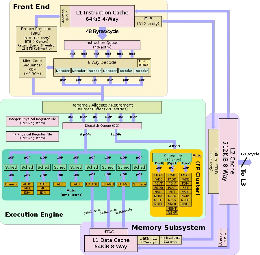
Individual Core
Memory Hierarchy
- Cache
- L1I Cache
- 64 KiB, 4-way set associative
- 128 B line size
- per core
- Parity-protected
- 64 KiB, 4-way set associative
- L1D Cache
- 64 KiB, 8-way set associative
- 64 B line size
- per core
- 4 cycles for fastest load-to-use
- 32 B/cycle load bandwidth
- 16 B/cycle store bandwidth
- 64 KiB, 8-way set associative
- L2 Cache
- 512 KiB, 8-way set associative
- Inclusive of L1
- 12 cycles latency
- 32 B/cycle bandwidth
- L3 Cache
- 4 MiB, 16-way set associative
- 1 MiB slice/core
- ~37-cycle typical (NUCA)
- 4 MiB, 16-way set associative
- BIU
- 80 outstanding transactions
- L1I Cache
Mongoose 1 TLB consists of dedicated L1 TLB for instruction cache (ITLB) and another one for data cache (DTLB). Additionally, there is a unified L2 TLB (STLB).
- TLBs
- ITLB
- 512-entry
- DTLB
- 32-entry
- 512-entry Mid-level DTLB
- STLB
- 4,096-entry
- Per core
- ITLB
- BPU
- 4K-entry main BTB
- 128-entry µBTB
- 64-entry return stack
- 16K-entry L2 BTB
Overview
The M3 was originally planned to be an incremental design over the original M1. Design for the M3 started in 2014 with RTL design starting in 2015. When started, the goals for the M3 were around 10-15% performance improvements and the polishing of low-hanging fruits that were left from their first generation design. Samsung stated that throughout the development cycle of the M3, goals were drastically changed for considerably higher performance along with a much wider and deeper pipeline. First M3-based product was productized in Q1 2018 on Samsung's own 10 nm process operating at 2.7 GHz.
Core
The M3 is an out-of-order microprocessor with a 6-way decode and a 12-way dispatch.
Front end
The front-end of the M3 is tasked with the prediction of future instruction streams, the fetching of instructions, and the code of the ARM instructions into micro-operations to be executed by the back-end.
Fetch & pre-decoding
With the help of the branch predictor, the instructions should already be found in the level 1 instruction cache. The L1I cache is 64 KiB, 4-way set associative. Samsung kept the L1I cache the same as prior generations. The L1I cache and has its own iTLB consisting of 512 entries, double the prior generation. A large change in the M3 is the instruction fetch bandwidth. Previously, up to 24 bytes could be read each cycle into the instruction queue. In the M3, now 48 bytes (up to 12 ARM instructions) are read each cycle into the instruction queue which allows them to hide very short branch bubbles and deliver a large number of instructions to be decoded by a larger decoder. The instruction queue is a slightly more complex component than a simple buffer. The byte stream gets split up into the ARM instructions its made off, including dealing with the various misaligned ARM instructions such as in the case of thumb mode. If the queue is filled to capacity, the fetch is gated for a cycle in order to allow the queue to naturally decrease.
Branch Predictor
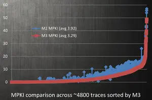
The M1 has a perceptron branch predictor with a couple of perceptrons which can handle two branches per cycle. The branch predictor on the M3 largely enhances the one found in the M1. A number of new weights were added and previous weights were re-tuned for various case accuracy. The unit is capable of indirect predictions as well as loop and stream predictions when it detects those traffic patterns. The indirect branches received a lot of attention in the M3. Additionally, the capacity of the micro-BTB was doubled to 128 entries which are used for caching very small tight loops and other hot kernels. Although the buffer size itself has not been increased, the average branch taken latency has also been improved through improvements of branch-taken turn-around time for various cases that could be expedited. The second-level BTB capacity was also doubled to 16K entries deep.
In total, Samsung reported a net reduction of the average miss-predictions per thousand instructions (MPKI) of around 15% (shown in the graph on the right) over the M2.
The branch predictor feeds a decoupled instruction address queue which in turn feeds the instruction cache.
Decoding
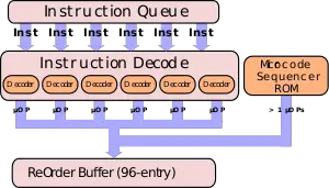
From the instruction queue the instructions are sent to decode. The decode unit on the M3 was increased significantly to 6-way (from 4), allowing up to six instructions to be decoded each cycle. The Decoder which can handle both the ARM AArch64 and AArch32 instructions. All in all, up to six µOPs are decoded and sent to the re-order buffer each cycle. One of the new features on the M3 is the introduction of some initial fusion idioms support which allows the decoder to decode two instructions and if they meet a certain criteria, they can be fused into a single µOP which remains that way for the remainder of the pipeline, alleviating various resources that would other require two entries.
Micro-Sequencer
For some complex ARM instructions such as the ARMv7 load-store multiples instructions which result in multiple µOPs being emitted, M3 has a side micro-sequencer that will get invoked and emit the appropriate µOPs.
Execution engine
Renaming & Allocation
As with the decode, up to six µOPs can be renamed each cycle. This is up from four µOPs in all the prior generations. For some special cases such as in ARMv7 where four single-precision registers can alias into a single quad register or a pair of doubles, the M3 has special logic in the rename area to handle the renaming of those floating point µOPs. For the case of a branch misprediction, the M3 has a perform fast map recovery ability as a branch misprediction recovery mechanism.
Matching the wider pipeline, the reoder buffer has been substantially increased in size to 228 µOPs that can be in flight. The ROB feeds the dispatch queue at the rate of up to 6 µOPs per cycle.
Dispatch
From the dispatch queue, up to 9 µOPs may be issued to the integer cluster and up to 3 µOPs may be issued to the floating point cluster. This is a large change from the M1 and M2 where up to 7 and 2 micro-operations could be sent to the integer and floating point clusters respectively.
Integer cluster
The dispatch queue feeds the execution units. The M3 doubles the physical register files. For integers, there is now a 192-entry integer physical register file (roughly 35-36 of them is architected) which means data movement is not necessary. In the integer execution cluster, up to 9 µOPs per cycle may be dispatched to the schedulers. The schedulers are distributed across the various pipes. M3 more than doubled the depth of those schedulers. In total, the integer schedulers now have 126 entries and those entries are distributed in mixed sizes across the 9 schedulers.
For the first pipe the M3, like it's predecessors, has a branch resolution unit. The next four pipes have integer ALUs. Whereas in the prior design there was one complex ALU pipe and three simple ALU pipes, in the M3 the newly added pipe is also a complex ALU. In other words, while all four pipes are capable of executing the typical integer ALU µOPs (i.e., two-source µOPs), only the ALUCs (complex ALUs) can also execute three source µOPs. This includes some of the ARMv7 special predicate forms. Generally speaking, most of the simple classes of instructions (e.g., normal add) should be a single cycle while the more complex operations (e.g., add with barrel shift rotate) would be a cycle or two more. Compared to the M1, Samsung was able to reduce the latency for some of the shift+add and similar µOPs down from two cycles to just one. For a few special cases, Samsung was also able to reduce the latency down to zero cycles.
For the integer divider unit, the M3 implements a radix 16 (4 bits/cycle), halving the latency in the iterative portion from the prior generation which implemented a radix 4 (2 bits/cycle) divider unit.
The last four pipes are for the AGUs and store data execution units (discussed later).
Floating-point cluster
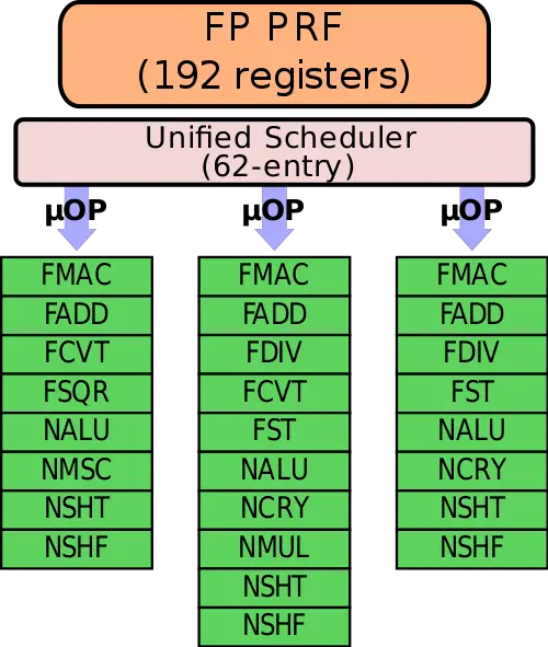
On the floating point cluster side, the adds another FP pipe and close to doubled the scheduler. Here, up to 3 µOPs may be issued to a unified scheduler which consists of 62 entries. Like the integer side, the FP FRP has also doubled in capacity with a 192-entry floating point (vector) physical register file (roughly 35-36 architected). There are three pipes and all three pipes have an integer SIMD unit (NEON).
The first pipe features a 4-cycle FMAC and a 3-cycle multiplier while the second pipe incorporates a 2-cycle floating-point adder. In all three units, Samsung reduced the latency by one cycle (from 5, 4, and 3 cycle latencies respectively). Overall, all three pipes are fuller and more capable. All three pipes have an FMAC and FADD units, doubling the FLOPS of the prior design. Additionally, there is a second pipe with a cryptography floating point conversion unit. Similar to the integer divider unit, the M3 also implements a radix 16 (4 bits/cycle) for the FDIV unit, halving the latency in the iterative portion from the prior generation which implemented a radix 4 (2 bits/cycle).
As with the integer cluster, there are now two pipes that incorporate a 128-bit floating point store/load port.
Retirement
Once execution is complete, µOPs may retire at a rate of up to 6 µOPs per cycle.
Memory subsystem
The memory subsystem on the M3 has been entirely overhauled. Whereas the M1 had a 32 KiB level 1 data cache, the M3 doubled it to 64 KiB. It's still 8-way set associative which is ECC protected. Loads and stores are done fully out of order with all the typical forwarding and light prediction that prevents thrashing.
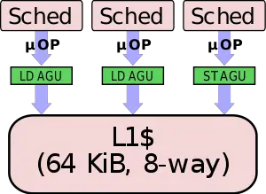
In the prior generations, the M1 was capable of a single 128-bit load each cycle and a single 128-bit store each cycle. The M3 supports two 128-bit loads each cycle and one 128-bit store per cycle. Note that both operations can be done at the same cycle. With the floating-point stores in ARM, the M3 can match and load-store bandwidth in many copy scenarios. Despite doubling the cache size, the level 1 data cache still maintains a 4-cycle load latency and can support 12 outstanding misses to the L2 hierarchy. Additionally, the M3 LSU schedulers are larger and the store buffer was doubled in capacity.
The M3 has a multi-stride prefetcher which allows it to detect patterns and start the fetching request ahead of execution. There is also some stream/copy optimizations as well which accelerate certain observable traffic patterns. In the M3, Samsung added new stream and copy optimizations. They also added new patterns to the prefetcher in order to address addition scenarios.
As with the M1, the dTLB is still 32 entries which remain considerably smaller than the 512-entry iTLB. The reason remains similar to that of the M1 which is because the front-end is designed with a lot more room in mind as far as handling a larger TLB capacity natively in its pipeline. It's also physically laid out much further on the floor plan. This allows the L2 TLB to service the dTLB more aggressively. The TLB on the M3 has been slightly remapped. In addition to the 32-entry primary dTLB, there is a new mid-level dTLB that's 512-entry deep. The second-level STLB has also quadrupled in size from 1K in the prior generation to 4K on the M3.
All M3 Processors
| List of M3-based Processors | |||||||
|---|---|---|---|---|---|---|---|
| Main processor | Integrated Graphics | ||||||
| Model | Family | Launched | Arch | Cores | Frequency | GPU | Frequency |
| Count: 0 | |||||||
Bibliography
- Template:hcbib
- LLVM: lib/Target/AArch64/AArch64SchedExynosM3.td
| codename | Mongoose 3 + |
| core count | 4 + |
| designer | Samsung + |
| first launched | 2018 + |
| full page name | samsung/microarchitectures/m3 + |
| instance of | microarchitecture + |
| instruction set architecture | ARMv8 + |
| manufacturer | Samsung + |
| microarchitecture type | CPU + |
| name | Mongoose 3 + |
| process | 10 nm (0.01 μm, 1.0e-5 mm) + |
