| Edit Values | |
| Kirin 970 | |
 | |
| General Info | |
| Designer | HiSilicon, ARM Holdings |
| Manufacturer | TSMC |
| Model Number | 970 |
| Market | Mobile |
| Introduction | September 1, 2017 (announced) September 1, 2017 (launched) |
| General Specs | |
| Family | Kirin |
| Series | 900 |
| Frequency | 1,800 MHz, 2,360 MHz |
| Microarchitecture | |
| ISA | ARMv8 (ARM) |
| Microarchitecture | Cortex-A53, Cortex-A73 |
| Core Name | Cortex-A53, Cortex-A73 |
| Process | 10 nm |
| Transistors | 5,500,000,000 |
| Technology | CMOS |
| Die | 96.72 mm² 9.75 mm × 9.92 mm |
| Word Size | 64 bit |
| Cores | 8 |
| Threads | 8 |
| Max Memory | 6 GiB |
| Multiprocessing | |
| Max SMP | 1-Way (Uniprocessor) |
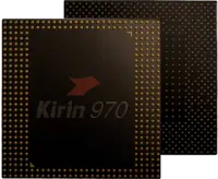
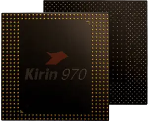
Kirin 970 is a 64-bit octa-core high-performance mobile ARM LTE SoC introduced by HiSilicon in mid-2017 at the 2017 IFA. This chip, which is fabricated on a 10 nm process, features four Cortex-A73 big cores operating at up to 2.36 GHz along with four Cortex-A53 little cores operating at up to 1.8 GHz. The 970 incorporates ARM's Mali G72 (12 core) IGP operating at 850 MHz and supports up to 6 GiB of dual-channel LPDDR4-1866 memory.
Contents
Overview
Introduced at the 2017 IFA, the overall core organization is identical to the Kirin 960 which was introduced the previous year, but features 20% power efficiency and 40% smaller die area due to the process shrink. The 970 ballooned to over 37.5% more transistors from 4 billion in the 960 to 5.5 billion. The 970 adds many enhancements, including a more powerful Mali G72 GPU and incorporates a new Neural Network Processing Unit (NPU) designed for AI acceleration. The 970 has two improved ISPs and a more powerful LTE modem supporting up to User Equipment (UE) category 18 capable of reaching a maximum downlink of 1.2 Gbps (4x4 MIMO, 256 QAM, 3CC CA).
Cache
- Main articles: Cortex-A53 § Cache and Cortex-A73 § Cache
|
Cache Organization
Cache is a hardware component containing a relatively small and extremely fast memory designed to speed up the performance of a CPU by preparing ahead of time the data it needs to read from a relatively slower medium such as main memory. The organization and amount of cache can have a large impact on the performance, power consumption, die size, and consequently cost of the IC. Cache is specified by its size, number of sets, associativity, block size, sub-block size, and fetch and write-back policies. Note: All units are in kibibytes and mebibytes. |
||
|
|
||
| This section requires expansion; you can help adding the missing info. |
Memory controller
|
Integrated Memory Controller
|
||||||||||||||||
|
||||||||||||||||
Graphics
|
Integrated Graphics Information
|
||||||||||||||||||||||||||||||||||
|
||||||||||||||||||||||||||||||||||
- Hardware Acceleration
- Decode: 2160p @ 60fps
- Encode: 2160p @ 30fps
Wireless
- LTE Modem
- Up to User Equipment (UE) category 18
- Downlink of up to 1.2 Gbps (4x4 MIMO, 256 QAM, 3CC CA)
- Uplink of up to 150 Mbps (2x20MHz CA, 64-QAM)
- Up to User Equipment (UE) category 18
- Wi-Fi 802.11 ac Dual Band
- Bluetooth 4.2
- NFC
- GPS / A-GPS / GLONASS / BDS
Expansions
- Dual ISPs
- 14-bit
Neural Network Processing Unit (NPU)
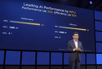
The Kirin 970 incorporates a new Neural Network Processing Unit (NPU) designed specifically to be used as an AI accelerator. According to CEO Richard Yu, who also introduced the processor at 2017 IFA, the NPU uses up the die area of roughly half of the CPU while consuming 50% less power and performing around 25 times faster than a traditional CPU for tasks such as photo recognition. The NPU is said to deliver 1.92 TFLOPs (HP 16-bit). While the exact architectural detials of the NPU have been withheld, the NPU appear to be a licensed IP design from Cambricon Technologies.
Utilizing devices
- Huawei Honor V10 (Honor View 10)
- Huawei P20
- Huawei P20 Pro
- Huawei P20 Lite
- Huawei Honor 10
- Huawei Mate 10 Pro
- Hikey970
- Huawei Honor Play
- Huawei Mate RS Porsche Design
- Huawei Mate 10 Porsche Design
This list is incomplete; you can help by expanding it.
- all microprocessor models
- microprocessor models by hisilicon
- microprocessor models by hisilicon based on cortex-a53
- microprocessor models by hisilicon based on cortex-a73
- microprocessor models by arm holdings
- microprocessor models by arm holdings based on cortex-a53
- microprocessor models by arm holdings based on cortex-a73
- microprocessor models by tsmc
| base frequency | 1,800 MHz (1.8 GHz, 1,800,000 kHz) + and 2,360 MHz (2.36 GHz, 2,360,000 kHz) + |
| core count | 8 + |
| core name | Cortex-A53 + and Cortex-A73 + |
| designer | HiSilicon + and ARM Holdings + |
| die area | 96.72 mm² (0.15 in², 0.967 cm², 96,720,000 µm²) + |
| die length | 9.75 mm (0.975 cm, 0.384 in, 9,750 µm) + |
| die width | 9.92 mm (0.992 cm, 0.391 in, 9,920 µm) + |
| family | Kirin + |
| first announced | September 1, 2017 + |
| first launched | September 1, 2017 + |
| full page name | hisilicon/kirin/970 + |
| has ecc memory support | false + |
| instance of | microprocessor + |
| integrated gpu | Mali-G72 + |
| integrated gpu base frequency | 850 MHz (0.85 GHz, 850,000 KHz) + |
| integrated gpu designer | ARM Holdings + |
| integrated gpu execution units | 12 + |
| isa | ARMv8 + |
| isa family | ARM + |
| ldate | September 1, 2017 + |
| main image |  + + |
| manufacturer | TSMC + |
| market segment | Mobile + |
| max cpu count | 1 + |
| max memory | 6,144 MiB (6,291,456 KiB, 6,442,450,944 B, 6 GiB, 0.00586 TiB) + |
| max memory bandwidth | 27.82 GiB/s (28,487.68 MiB/s, 29.871 GB/s, 29,871.498 MB/s, 0.0272 TiB/s, 0.0299 TB/s) + |
| max memory channels | 2 + |
| microarchitecture | Cortex-A53 + and Cortex-A73 + |
| model number | 970 + |
| name | Kirin 970 + |
| process | 10 nm (0.01 μm, 1.0e-5 mm) + |
| series | 900 + |
| smp max ways | 1 + |
| supported memory type | LPDDR4-1866 + |
| technology | CMOS + |
| thread count | 8 + |
| transistor count | 5,500,000,000 + |
| used by | Huawei Honor V10 (Honor View 10) +, Huawei P20 +, Huawei P20 Pro +, Huawei P20 Lite +, Huawei Honor 10 +, Huawei Mate 10 Pro +, Hikey970 +, Huawei Honor Play +, Huawei Mate RS Porsche Design + and Huawei Mate 10 Porsche Design + |
| word size | 64 bit (8 octets, 16 nibbles) + |
