| Edit Values | |
| Gen9 LP µarch | |
| General Info | |
| Arch Type | GPU |
| Designer | Intel |
| Manufacturer | Intel |
| Introduction | August 5, 2015 |
| Process | 14 nm |
| Succession | |
Gen9 LP (Generation 9 Low Power) is the microarchitecture for Intel's graphics processing unit utilized by Skylake-based microprocessors. Gen9 LP is the successor to Gen8 LP used by Broadwell. The Gen9 microarchitecture is designed separately by Intel and then integrated onto the same Skylake SoC die.
Contents
Codenames
Various models support different Graphics Tiers (GT) which provides different levels of performance. Some models also support an additional eDRAM side cache.
| Code Name | Description |
|---|---|
| GT1 | Contains 1 slice with 12 execution units. |
| GT2 | Contains 1 slice with 24 execution units. |
| GT3 | Contains 2 slices with 48 execution units. |
| GT3e | Contains 2 slices with 48 execution units. Has an additional eDRAM side cache. |
| Halo (GT4e) | Contains 3 slices with 72 execution units. Has an additional eDRAM side cache. |
Models
| Gen9 LP IGP Models | Standards | ||||||||||||
|---|---|---|---|---|---|---|---|---|---|---|---|---|---|
| Name | Execution Units | Tier | Series | eDRAM | Vulkan | Direct3D | OpenGL | OpenCL | |||||
| Windows | Linux | Windows | Linux | HLSL | Windows | Linux | Windows | Linux | |||||
| HD Graphics (Skylake) | 12 | GT1 | Y | - | 1.0 | 12 | N/A | 5.1 | 4.4 | 4.5 | 2.0 | ||
| HD Graphics 510 | 12 | GT1 | U, S | - | |||||||||
| HD Graphics 515 | 24 | GT2 | Y | - | |||||||||
| HD Graphics 520 | 24 | GT2 | U | - | |||||||||
| HD Graphics 530 | 24 | GT2 | H, S | - | |||||||||
| HD Graphics P530 | 24 | GT2 | H | - | |||||||||
| Iris Graphics 540 | 48 | GT3e | U | 64 MiB | |||||||||
| Iris Graphics 550 | 48 | GT3e | U | 64 MiB | |||||||||
| Iris Pro Graphics 580 | 72 | GT4e | H | 128 MiB | |||||||||
Hardware Accelerated Video
| [Edit] Skylake (Gen9) Hardware Accelerated Video Capabilities | |||||||
|---|---|---|---|---|---|---|---|
| Codec | Encode | Decode | |||||
| Profiles | Levels | Max Resolution | Profiles | Levels | Max Resolution | ||
| MPEG-2 (H.262) | Main | High | 1080p (FHD) | Main | Main, High | 1080p (FHD) | |
| MPEG-4 AVC (H.264) | High, Main | 5.1 | 2160p (4K) | Main, High, SHP, MHP | 5.1 | 2160p (4K) | |
| JPEG/MJPEG | Baseline | - | 16k x 16k | Baseline | Unified | 16k x 16k | |
| HEVC (H.265) | Main | 5.1 | 2160p (4K) | Main, Main 10 | 5.1 | 2160p (4K) | |
| VC-1 | ✘ | Advanced, Main, Simple | 3, High | 3840x3840 | |||
| VP8 | Unified | Unified | - | 0 | Unified | 1080p | |
| VP9 | ✘ | 0 | Unified | 2160p (4K) | |||
Process Technology
- Main article: Broadwell § Process Technology
Gen9 LP are part of the Skylake SoC die which uses the same 14 nm process used for the Broadwell microarchitecture.
Architecture
Gen9 LP presents a large departure from the Gen8 LP and previous architectures.
Key changes from Gen8 LP
- Architecture is drastically different
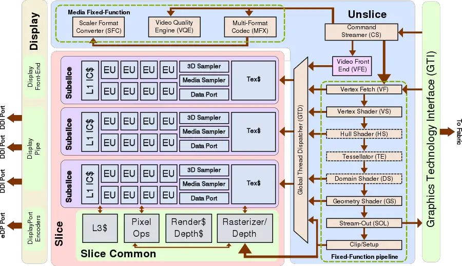
- Gen9 LP is composed of 3 truely independent major components: Display block, Unslice, and the Slice.
- Unslice
- Now sits on its own power gating/clock domain
- Capable of running at higher speeds if the situation allows (irrespective of slice clock)
- Can allow for pure fixed media alone
- Higher throughput
- Tessellator AutoStrip
- Fixed function video encoder in the Quick Sync engine
- codec (decode&encode) support for HEVC, VP8, MJPEG
- RAW imaging capabilities
- Now sits on its own power gating/clock domain
- Slice
- L3 Cache
- Increased to 768 KiB/slice (up from 576 KiB/slice)
- Request queue size was increased
- L3 Cache
- Subslice
- Adaptive scalable texture compression (ASTC)
- 16x multi-sample anti-aliasing (MSAA)
- Post depth test coverage mask
- Multi-plane overlays
- Texture samplers now natively support an NV12 YUV
- Preemption of execution is now supported at the thread level
- Round robin scheduling of threads within an execution unit.
- new native support for the 32-bit float atomics operations of min, max, and compare/exchange.
- 16-bit floating point capability is improved with native support for denormals and gradual underflow
- L4$
- The eDRAM is now a side cache instead of an L4$ like it was in Gen8 LP. (See Skylake §eDRAM architectural changes for the reason)
- Side-cache eDRAM was moved into the system agent adjacent to the display controller
Block Diagram
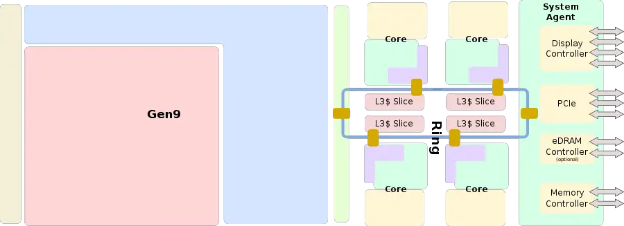
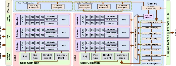
Entire SoC Overview
Gen9 LP
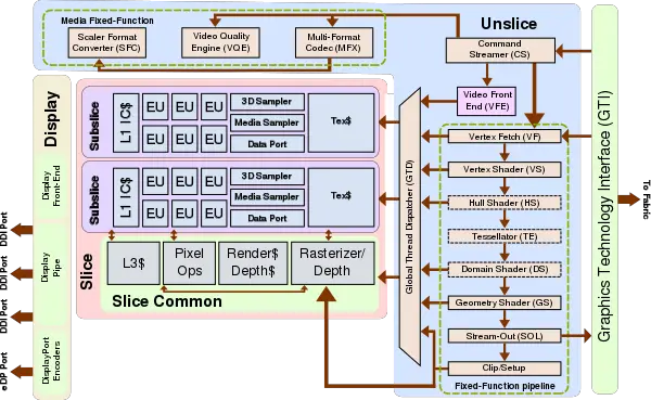
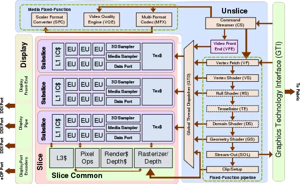
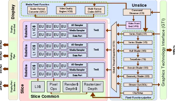
This block is for the most common setup, which is GT2 with 24 execution units.
Individual Core
Display
| This section is empty; you can help add the missing info by editing this page. |
Unslice
The Unslice is one of Gen9's major components and is responsible for the fixed-function geometry capabilities, fixed-function media capabilities, and it provides the interface to the memory fabric. One of the big changes in Gen9 is that the Unslice now sits on its own power/clock domain. This change allows the Unslice to operate at its own speed provided higher on-demand performance when desired. This change has a number of other benefits such as being able to turn off the slices (one or more) when they're not used in cases where pure fixed-function media is used. Additionally, the Unslice is now capable of running at a higher clock while the slice can run at a slower clock when the scenario demands it (such as in cases where higher fixed-function geometry or memory demands occur).
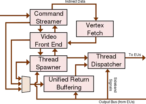
The Command Stream (CS) unit manages the the flow of execution for the FF Pipeline (3D Pipeline) and the Media pipelines. The CS unit performs the switching between pipelines and forwarding command streams to the different stages. Data in the pipeline are passed to the next unit using a messaging network. Messages can be passed directly through registers or by using the URB. The Command Stream also manages the allocation of the URB and supports the Constant URB Entry (CURB) function. The Unified Return Buffer (URB) is globally shared and is explicitly addressed. The pipeline's fixed-function blocks have both read and write access to the URB, additionally the shader cores have write access to the URB.
The media general-purpose pipeline consists of two fixed-function units: Video Front End (VFE) and the Thread Spawner (TS). The VFE unit handles the interfacing with the Command Streamer, writes thread payload data into the Unified Return Buffer, as well as prepares threads to be dispatched through TS unit. The VFE unit also contains the hardware Variable Length Decode (VLD) engine for MPEG-2 video decode. The TS unit is primarily responsible for interfacing with the Thread Dispatcher (TD) unit which is responsible for spawning new root-node parent threads originated from VFE unit and for spawning child threads (either leaf-node child threads or branch-node parent thread).
3D Pipeline Stages
| Pipeline Stage | Functions Performed |
|---|---|
| Command Stream (CS) | The Command Stream stage is responsible for managing the 3D pipeline and passing commands down the pipeline. In addition, the CS unit reads “constant data” from memory
buffers and places it in the URB. Note that the CS stage is shared between the 3D, GPGPU and Media pipelines. |
| Vertex Fetch (VF) | The Vertex Fetch stage, in response to 3D Primitive Processing commands, is responsible for reading vertex data from memory, reformatting it, and writing the results into Vertex URB Entries. It then outputs primitives by passing references to the VUEs down the pipeline. |
| Vertex Shader (VS) | The Vertex Shader stage is responsible for processing (shading) incoming vertices by passing them to VS threads. |
| Hull Shader (HS) | The Hull Shader is responsible for processing (shading) incoming patch primitives as part of the tessellation process. |
| Tessellation Engine (TE) | The Tessellation Engine is responsible for using tessellation factors (computed in the HS stage) to tessellate U,V parametric domains into domain point topologies.
Domain Shader (DS) The Domain Shader stage is responsible for processing (shading) the domain points (generated by the TE stage) into corresponding vertices. |
| Geometry Shader (GS) | The Geometry Shader stage is responsible for processing incoming objects by passing each object’s vertices to a GS thread. |
| Stream Output Logic (SOL) | The Stream Output Logic is responsible for outputting incoming object vertices into Stream Out Buffers in memory. |
| Clipper (CLIP) | The Clipper stage performs Clip Tests on incoming objects and clips objects if required. Objects are clipped using fixed-function hardware |
| Strip/Fan (SF) | The Strip/Fan stage performs object setup. Object setup uses fixed-function hardware. |
| Windower/Masker (WM) | The Windower/Masker performs object rasterization and determines visibility coverage |
Slice
Slices are a cluster of subslices. For most configurations in Gen9, 3 subslices are aggregated into 1 slice to form a total of 24 execution units (depending on the model, some low end models do have less). The slice incorporates the thread dispatch routine, level 3 cache (L3$), a highly banked shared local memory structure, fixed function logic for atomics and barriers, and a number of fixed-function units for various media capabilities. The Global Thread Dispatcher (GTD) is responsible for load balancing thread distribution across the entire device. The global thread dispatcher works in concert with local thread dispatchers in each subslice.
Execution Unit (EU)
| This section is empty; you can help add the missing info by editing this page. |
Scalability
Gen9 can scale from 1 to 3 slices producing SKUs ranging from 12 to 72 execution units (note that the 12 EUs are formed from half a slice effectively).
GT1 (ULP)
GT1 is the most compact configuration offering two benefits: reduced cost and reduced power. GT1 is made of 1 slice containing 2 subslices with 6 EUs/subslice for a total of 12 EUs. With the scale-down, GT1 changes the ratio to 6:1 EU:sampler ratio. Note that this does retains the same ratio of 12 texels/clock and 8 pixels/clock at the backend. This configuration is better suited for some of the low power worlkload (e.g. ASTC-LDR+HDR, ETC1/2 compression). Note that software stack remains unchanged compared to the larger models.
GT1.5
GT1.5, offers 3 subslices of 6 EUs each for a total of 18 EUs.
GT2
GT2 is the standard configuration consisting of 1 slice with 3 subslices and 8 EU/subslice for a total of 24 EUs.
GT3
GT3 consists of 2 slices with 3 subslices in each and 8 EU/subslice for a total of 48 EUs.
Halo (GT4)
Codename Halo (GT4) is the most complex configuration offering the highest execution units count. Halo incorporates 3 slices with 3 subslices/slice and 8 EU/subslice for a total of 72 EUs.
Configuration
| Product Configuration Attribute Table (Source: Intel) | ||||||
|---|---|---|---|---|---|---|
| Attribute | Model | |||||
| GT1F (1x2x6) |
GT1.5F (1x3x6) |
GT2 (1x3x8) |
GT3 (2x3x8) |
GT4 (3x3x8) | ||
| codename | Gen9 LP + |
| designer | Intel + |
| first launched | August 5, 2015 + |
| full page name | intel/microarchitectures/gen9 + |
| instance of | microarchitecture + |
| manufacturer | Intel + |
| microarchitecture type | GPU + |
| name | Gen9 LP + |
| process | 14 nm (0.014 μm, 1.4e-5 mm) + |
