| Edit Values | |
| Cortex-A77 µarch | |
| General Info | |
| Arch Type | CPU |
| Designer | ARM Holdings |
| Manufacturer | TSMC, samsung, SMIC |
| Introduction | May 27, 2019 |
| Process | 10 nm, 7 nm, 5 nm |
| Core Configs | 1, 2, 4, 6, 8 |
| Pipeline | |
| Type | Superscalar, Pipelined |
| OoOE | Yes |
| Speculative | Yes |
| Reg Renaming | Yes |
| Stages | 13 |
| Decode | 4-way |
| Instructions | |
| ISA | ARMv8.2 |
| Extensions | FPU, NEON |
| Cache | |
| L1I Cache | 64 KiB/core 4-way set associative |
| L1D Cache | 64 KiB/core 4-way set associative |
| L2 Cache | 128-512 KiB/core 8-way set associative |
| L3 Cache | 0-4 MiB/Cluster 16-way set associative |
| Succession | |
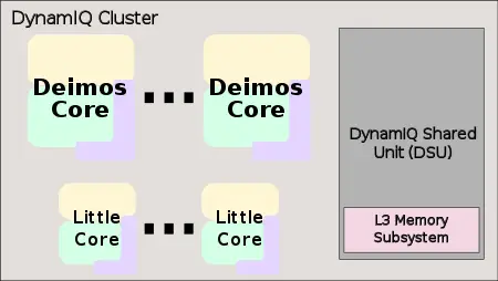
Cortex-A77 (codename Deimos) is the successor to the Cortex-A76, a low-power high-performance ARM microarchitecture designed by ARM Holdings for the mobile market. Deimos was designed by Arm's Austin, Texas team. This microarchitecture is designed as a synthesizable IP core and is sold to other semiconductor companies to be implemented in their own chips. The Cortex-A77, which implemented the ARMv8.2 ISA, is a high performance core which is often combined with a number of low(er) power cores (e.g. Cortex-A55) in a DynamIQ big.LITTLE configuration to achieve better energy/performance.
Contents
History[edit]
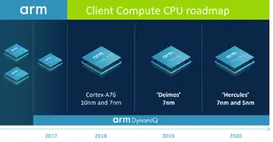
Development of the Cortex-A77 started in 2014. Arm formally announced Deimos during Computex on May 27 2019.
Process Technology[edit]
Though the Cortex-A77 may be fabricated on various different process nodes, it has been primarily designed for the 10 nm, 7 nm, and 5 nm process nodes.
Compiler support[edit]
| Compiler | Arch-Specific | Arch-Favorable |
|---|---|---|
| Arm Compiler | -mcpu=cortex-a77 |
-mtune=cortex-a77
|
| GCC | -mcpu=cortex-a77 |
-mtune=cortex-a77
|
| LLVM | -march=cortex-a77 |
-mtune=cortex-a77
|
If the Cortex-A77 is coupled with the Cortex-A55 in a big.LITTLE system, GCC also supports the following option:
| Compiler | Tune |
|---|---|
| GCC | -mtune=cortex-a77.cortex-a55
|
Architecture[edit]
Key changes from Cortex-A76[edit]
- Performance
- IPC uplift (Arm self-reported around 20% IPC on SPEC CPU2006/SPEC CPU2017 int)
- Front-end
- Branch-prediction
- Improved accuracy
- 2x larger runahead window (64B, up from 32B)
- 1.33x larger BTB capacity (8K-entry, up from 6K)
- 4x larger L1 BTB capacity (64-entry, up from 16)
- Improved prefetcher
- New L0 MOP cache
- 1.5x wider instruction fetch (6 instrs/cycle, up from 4)
- Branch-prediction
- Execution engine
- 1.5x wider instruction fetch (6 instrs/cycle, up from 4)
- 1.0x wider decode (4-way)
- 1.5x wider rename/comit (6-way, up from 4-way)
- lower latency recovery from branch mispredict flushes
- 1.25x larger ROB (160-entry, up from 128)
- 1.25x wider dispatch (10-way, up from 8-way)
- 1.5x wider issue (12-way, up from 8-way)
- Execution units
- issue queue (IQ) is now unified for integers
- issue queue (IQ) is now unified for floating points
- New integer ALU unit and port
- New branch unit and port
- New dedicated store data ports
- New AES unit added
- Execution units
- Memory subsystem
- issue queue (IQ) is now unified for the memory subsystem
- 1.25 larger load buffer (85-entry, up from 68)
- 1.25 larger store buffer (90-entry, up from 72)
- 2x load/store issue bandwidth
- Improved prefetcher
- System-aware prefetching
- Improved tolerance to varying memory subsystem implementations
- Dynamic distance/aggressiveness
This list is incomplete; you can help by expanding it.
Block Diagram[edit]
Typical SoC[edit]
Individual Core[edit]
Memory Hierarchy[edit]
The Cortex-A77 has a private L1I, L1D, and L2 cache.
- Cache
- L0 MOP Cache
- 1536-entry
- L1I Cache
- 64 KiB, 4-way set associative
- 64-byte cache lines
- Optional parity protection
- Write-back
- L1D Cache
- 64 KiB, 4-way set associative
- 64-byte cache lines
- 4-cycle fastest load-to-use latency
- Optional ECC protection per 32 bits
- Write-back
- L2 Cache
- 256 KiB OR 512 KiB (2 banks)
- 8-way set associative
- 9-cycle fastest load-to-use latency
- optional ECC protection per 64 bits
- Modified Exclusive Shared Invalid (MESI) coherency
- Strictly inclusive of the L1 data cache & non-inclusive of the L1 instruction cache
- Write-back
- L3 Cache
- 2 MiB to 4 MiB, 16-way set associative
- 26-31 cycles load-to-use
- Shared by all the cores in the cluster
- located in the DynamIQ Shared Unit (DSU)
- L0 MOP Cache
The A77 TLB consists of dedicated L1 TLB for instruction cache (ITLB) and another one for data cache (DTLB). Additionally, there is a unified L2 TLB (STLB).
- TLBs
- ITLB
- 4 KiB, 16 KiB, 64 KiB, 2 MiB, and 32 MiB page sizes
- 48-entry fully associative
- DTLB
- 48-entry fully associative
- 4 KiB, 16 KiB, 64 KiB, 2 MiB, and 512 MiB page sizes
- STLB
- 1280-entry 5-way set associative
- ITLB
Overview[edit]
The Cortex-A77, formerly Deimos, is a high-performance synthesizable core designed by Arm as the successor to the Cortex-A76. It is delivered as Register Transfer Level (RTL) description in Verilog and is designed to be integrated into customer's SoCs. This core supports the ARMv8.2 extension as well as a number of other partial extensions. The Cortex-A77 is built on the extensive design work that was done on the A76 but enhances it in order to extract a significant amount of IPC while maintaining the same frequency range. To that end, the A77 is a 6-way superscalar out-of-order processor with a 12-wide execution engine, a private level 1, and level 2 caches. It is designed to be implemented inside the DynamIQ Shared Unit (DSU) cluster along with other cores. The DSU cluster supports up to eight cores of any combination (e.g., with little cores such as the Cortex-A55 or other just more Cortex-A77s).
Core[edit]
The Cortex-A77 succeeds the Cortex-A76. Like the A76, the A77 targets the 7 nm process but features an extensive set of changes designed to maximize the IPC while maintaining the same frequency range. Arm achieved this through the extraction of significant instruction-level parallelism through a much wider pipeline.
Pipeline[edit]
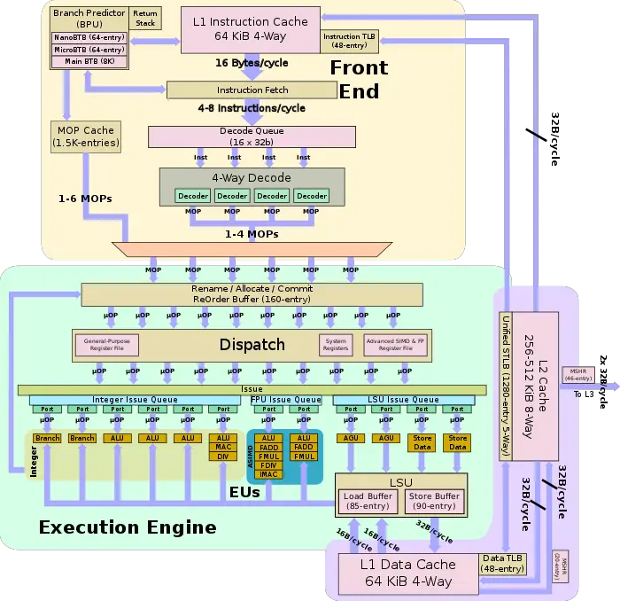
The Cortex-A77 is a complex, 6-way superscalar out-of-order processor with a 10-issue back end. The pipeline is 13 stages with an 10-cycle branch misprediction penalty best-case. It has a 64 KiB level 1 instruction cache and a 64 KiB level 1 data cache along with a private level 2 cache that is configurable as either 256 KiB (1 bank) or 512 KiB (2 banks).
Front-end[edit]
Each cycle, up to 32 bytes are fetched from the L1 instruction cache. The instruction fetch works in tandem with the branch predictor in order to ensure the instruction stream is constantly ready to be fetched. Additionally, there is a return stack which stores the address and instruction set state (AArch32/R14 or AArch64/X30) on branches. On a return (e.g., ret on AArch64), the return stack will pop.
Keeping the instruction stream feed is the task of the branch prediction unit. Like the Enyo, the branch prediction unit on Deimos is decoupled from the instruction fetch, allowing it to run ahead and in parallel with the instruction fetch to hide branch prediction latency. Since the instruction fetch has been increased, Arm also doubled the branch predictor instruction window size to 64 bytes/cycle, in order to allow it to runahead of the instruction stream. The main branch target buffer on the A77 has been increased by 33% compared to A76. It is now 8K-entries deep which Arm says directly improves the real-world performance of many workloads. The BPU comprises three stages in order to reduce latency with a 64-entry micro-BTB and a smaller 64-entry nano BTB which has been quadrupled in size from 16 entries in the A76.
Deimos has a fixed 64 KiB L1I cache. It is virtually indexed, physically tagged (VIPT), which behaves as a physically indexed, physically tagged (PIPT) 4-way set-associative cache. The L1I$ supports optional parity protection and implements a pseudo-LRU cache replacement policy. The instruction cache has a 256-bit read interface from the L2 cache. Each cycle up to 16 bytes may be transferred to the L1I cache from the shared L2 cache.
From the instruction fetch, up to four 32-bit instructions are sent to the decode queue (DQ) each cycle. This is two additional instructions per cycle more than the Enyo and is the widest pipeline Arm designed to that point. For narrower 16-bit instructions (i.e., Thumb), this means up to eight instructions get queued. The A76 features a 6-way decode. Each cycle, up to four instructions may be decoded into a relatively semi-complex macro-operations (MOPs). There are on average 6% more MOPs than instructions. In total two cycles are involved in this operation - one for alignment and one for decode.
Back-end[edit]
Deimos back-end handles the execution of out-of-order operations. The design is largely inherited from the Cortex-A76 but has been made considerably wider and deeper.
Renaming & Allocation[edit]
From the front-end, up to six macro-operations may be sent each cycle to be renamed. Deimos has a capacity to handle up to 160 instructions inflight, making it 25% wider than all its predecessors going all the way back to the Cortex-A57. Historically, Arm always explained that an increase in roughly 10 percent to reorder buffer results in just 1-1.25% in performance. With an increase of 25% on Deimos, this translates to roughly 2.5-3% in performance is extracted. The Micro-operations are broken down into their µOP constituents and are scheduled for execution. Roughly 20% more µOPs are generated from the MOPs. From here, µOPs are sent to the instruction issue which controls when they can be dispatched to the execution pipelines. µOPs are queued in eight independent issue queues (120 entries in total).
Execution Units[edit]
Deimos backend issue is 12-wide, an increase of 50% over Enyo. This allows for up to twelve µOPs to execute each cycle - 10 µOPs to the execution units and 2 store data points. The execution units on Deimos are grouped into three clusters: integer, advanced SIMD, and memory.
There are six pipelines in the integer cluster - an increase of two additional integer pipelines from Enyo. One of the changes from Enyo is the unification of the issue queues. Previously each pipeline had its own issue queue. On Deimos, there is now a single unified issue queue which improves efficiency. Deimos added a new fourth general math ALU with a typical 1-cycle simple math operations and some 2-cycle more complex operations. In total, there are three simple ALUs that perform arithmetic and logical data processing operations and a fourth port which has support for complex arithmetic (e.g. MAC, DIV). Deimos also added a second branch ALU, doubling the throughput for branches.
There are two ASIMD/FP execution pipelines. This is unchanged from Enyo. What did change is the issue queues. As with the integer cluster, the ASIMD cluster now features a unified issue queue for both pipelines, improving efficiency. As with Enyo, the ASIMD on Deimos are both 128-bit wide capable of 2 double-precision operations, 4 single-precision, 8 half-precision, or 16 8-bit integer operations. Those pipelines can also execute the cryptographic instructions if the extension is supported (not offered by default and requires an additional license from Arm). Versus Enyo, Deimos added a second AES unit in order to improve the throughput of cryptography operations.
Memory subsystem[edit]
Deimos includes two ports with an address-generation unit on each - each supporting both loads and stores. A large change in the A77 is how store-data is handled. Previously the two store-data pipelines shared the same issue ports as the integer ALUs. In Deimos, the two store-data pipelines now sit on their own dedicated ports, doubling the load-store issue bandwidth.
The level 1 data cache is fixed at 64 KiB and can have an optional ECC protection per 32 bits. It is virtually indexed, physically tagged which behaves as a physically indexed, physically tagged 4-way set-associative cache. The L1D cache implements a pseudo-LRU cache replacement policy. It features a 4-cycle fastest load-to-use latency with two read ports and one write port meaning it can do two 16B loads/cycle and one 32B store/cycle. From the L1, the A77 supports up to 20 outstanding non-prefetch misses. The load buffer is 85 entries deep while the store buffer is 90-entry deep. In total, Deimos can have 175 simultaneous memory operations in-flight which is roughly 10% more than the A77 instruction window.
The A77 can be configured with either 128, 256 or 512 KiB of level 2 cache with the two 265 KiB banks. It implements a dynamic biased replacement policy and is ECC protected per 64 bits. The L2 is strictly inclusive of the L1 data cache and non-inclusive of the L1 instruction cache. There is a 256-bit write interface to the L2 and a 256-bit read interface from the L2 cache. The fastest load-to-use latency is 9 cycles. The L2 can support up to 46 outstanding misses to the L3 which is located in the DSU itself. The L3, which is shared by all the cores in the DynamIQ big.LITTLE and is configurable in size ranging from 2 MiB to 4 MiB with load-to-use ranging from 26 to 31 cycles. As with the L2, up to two 32 bytes may be transferred from or to the L2 from the L3 cache. Up to 94 outstanding misses are supported from the L3 to main memory.
In addition to controlling memory accesses, ordering, and cache policies, the MMU is also responsible for the translation of virtual addresses to physical addresses on the system. This is done through a set of virtual-to-physical address mappings and attributes that are held in translation tables. The physical address size here is 40 bits. The Cortex-A77 incorporates a dedicated L1 TLB for instruction cache and another one for the data cache. Both the ITLB and the DTLB are 48-entry deep and are fully associative. On a memory access operation, the A77 will first perform lookup in there. If there is a miss in the L1 TLBs, the MMU will perform a lookup for the requested entry in the second-level TLB.
There is a unified level 2 TLB comprising of 1280 entries organized as 5-way set associative which is shared by both instruction and data. The STLB handles misses from the instruction and data L1 TLBs. Typically, STLB accesses take three cycles, however, longer latencies are possible when a different block or page size mapping is used. If there is a miss in the L2 TLB, the MMU will resort to a hardware translation table walk. Up to four TLB misses (i.e., translations table walks) can be performed in parallel. The STLB will stall if there are six successive misses. During table walks, the STLB can still perform up to two TLB lookups.
The TLB entries store one or both of the global indicator and an address space identifier (ASID), allowing context switching without TLB invalidation as well as a virtual machine identifier (VMID) which allows for VM switching by the hypervisor without TLB invalidation.
All Cortex-A77 Processors[edit]
| List of Cortex-A77-based Processors | ||||||||
|---|---|---|---|---|---|---|---|---|
| Main processor | Integrated Graphics | |||||||
| Model | Family | Launched | Process | Arch | Cores | Frequency | GPU | Frequency |
| 1000 | Dimensity | 2020 | 7 nm 0.007 μm 7.0e-6 mm | Cortex-A77, Cortex-A55 | 8 | 2.6 GHz 2,600 MHz , 2 GHz2,600,000 kHz 2,000 MHz 2,000,000 kHz | Mali-G77 | 836 MHz 0.836 GHz 836,000 KHz |
| 1000+ | Dimensity | 2020 | 7 nm 0.007 μm 7.0e-6 mm | Cortex-A77, Cortex-A55 | 8 | 2.6 GHz 2,600 MHz , 2 GHz2,600,000 kHz 2,000 MHz 2,000,000 kHz | Mali-G77 | |
| 1000L | Dimensity | 2020 | 7 nm 0.007 μm 7.0e-6 mm | Cortex-A77, Cortex-A55 | 8 | 2.2 GHz 2,200 MHz , 2 GHz2,200,000 kHz 2,000 MHz 2,000,000 kHz | Mali-G77 | |
| SDM865 | Snapdragon 800, Snapdragon 8 | March 2020 | 7 nm 0.007 μm 7.0e-6 mm | Cortex-A77, Cortex-A55 | 8 | 2.42 GHz 2,420 MHz , 2.84 GHz2,420,000 kHz 2,840 MHz , 2.1 GHz2,840,000 kHz 2,100 MHz 2,100,000 kHz | Adreno 650 GPU | 257 MHz 0.257 GHz 257,000 KHz |
| Count: 4 | ||||||||
Bibliography[edit]
- Arm Tech Day, 2019.
- Arm. personal communication. 2019.
Documents[edit]
| codename | Cortex-A77 + |
| core count | 1 +, 2 +, 4 +, 6 + and 8 + |
| designer | ARM Holdings + |
| first launched | May 27, 2019 + |
| full page name | arm holdings/microarchitectures/cortex-a77 + |
| instance of | microarchitecture + |
| instruction set architecture | ARMv8.2 + |
| manufacturer | TSMC +, samsung + and SMIC + |
| microarchitecture type | CPU + |
| name | Cortex-A77 + |
| pipeline stages | 13 + |
| process | 10 nm (0.01 μm, 1.0e-5 mm) +, 7 nm (0.007 μm, 7.0e-6 mm) + and 5 nm (0.005 μm, 5.0e-6 mm) + |


