| Edit Values |
| Gen9 LP µarch |
|
| Arch Type | GPU |
| Designer | Intel |
| Manufacturer | Intel |
| Introduction | August 5, 2015 |
| Process | 14 nm |
|
|
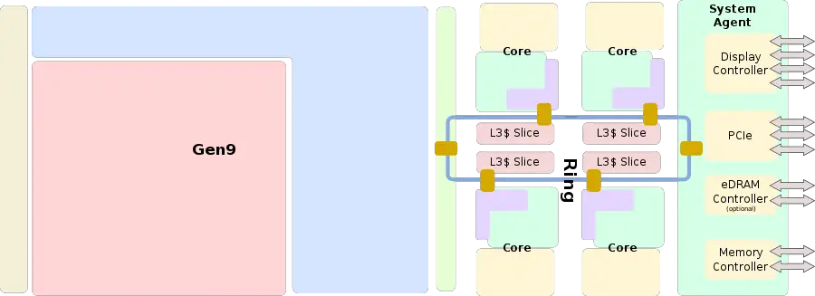
Gen9 LP (Generation 9 Low Power) is the microarchitecture for Intel's graphics processing unit utilized by Skylake-based microprocessors. Gen9 LP is the successor to Gen8 LP used by Broadwell. The Gen9 microarchitecture is designed separately by Intel and then integrated onto the same Skylake SoC die.
Architecture
Gen9 LP presents a large departure from the Gen8 LP and previous architectures.
Key changes from Gen8 LP
- Architecture is drastically different
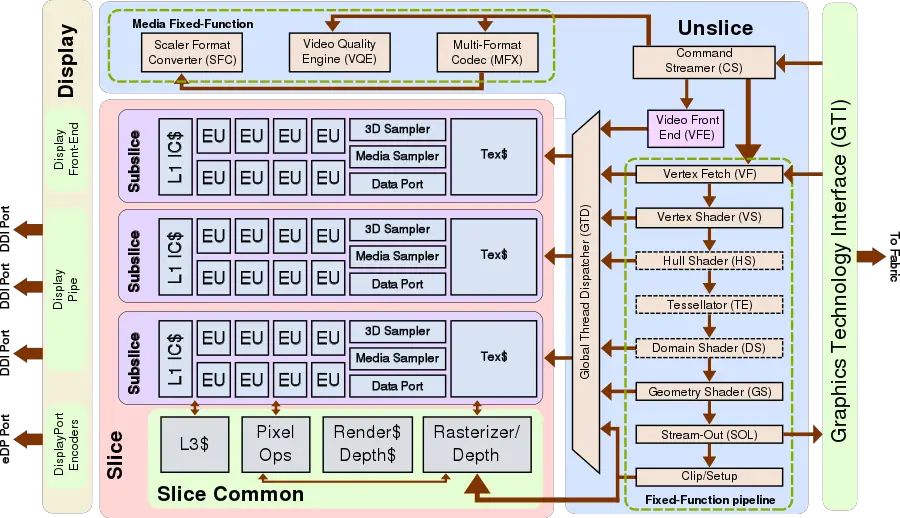
- Gen9 LP is composed of 3 truely independent major components: Display block, Unslice, and the Slice.
- Unslice
- Now sits on its own power/clock domain
- Capable of running at higher speeds if the situation allows (irrespective of slice clock)
- Can allow for pure fixed media alone
- Fixed-function geometry
- Higher throughput
- Tessellator AutoStrip
Block Diagram
Entire SoC Overview

Gen9 LP

Individual Core
See Skylake#Individual_Core.
Display
Unslice
The Unslice is one of Gen9's major components and is responsible for the fixed-function geometry capabilities, fixed-function media capabilities, and it provides the interface to the memory fabric. One of the big changes in Gen9 is that the Unslice now sits on its own power/clock domain. This change allows the Unslice to operate at its own speed provided higher on-demand performance when desired. This change has a number of other benefits such as being able to turn off the slices (one or more) when they're not used in cases where pure fixed-function media is used. Additionally, the Unslice is now capable of running at a higher clock while the slice can run at a slower clock when the scenario demands it (such as in cases where higher fixed-function geometry or memory demands occur).
Slice

