| Buffer Gate | |
|---|---|
| A | Q |
| 0 | 0 |
| 1 | 1 |
A buffer, is a basic logic gate that passes its input, unchanged, to its output. It's behavior is the opposite of a NOT gate. The main purpose of a buffer is to regenerate the input, usually using a strong high and a strong low. A buffer has one input and one output; its input always equals its input. Buffers are also used to increase the propagation delay of circuits by driving the large capacitive loads.
Standard symbol
Buffers are typically drown on schematics using one of the three standard symbols:
| ANSI | IEC | DIN |
|---|---|---|
 |
 |

|
CMOS Implementation
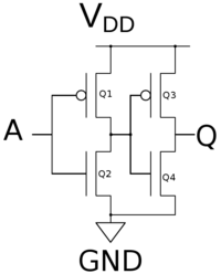
A CMOS buffer gate with one input and one output can be realized as simply two inverters back to back - built out of just 4 gates.
The table on the right shows the states of the four transistors with the various inputs of A.
| Buffer Gate by Transistor | |||||
|---|---|---|---|---|---|
| A | Q1 | Q2 | Q3 | Q4 | Q |
| 0 | 1 | 0 | 0 | 1 | 0 |
| 1 | 0 | 1 | 1 | 0 | 1 |
7407: Hex Buffer/Driver
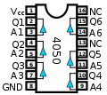
The 7407 is a TTL chip with 14 pins. Two pins are used for VDD and GND, the other 12 pins are used for the 6 independent buffers. The 4050 is a CMOS Hex Buffer with 16 pins. Two pins are used for VDD and GND, 12 pins are used for the 6 independent buffers. Pins 13 and 16 are not connected. Both chips implement the expression QN = AN


