| Edit Values | |
| Pixel Visual Core | |
| General Info | |
| Designer | |
| Manufacturer | TSMC |
| Part Number | X726C502 |
| S-Spec | SR3HX |
| Market | Mobile, Embedded |
| Introduction | October 17, 2017 (announced) October 17, 2017 (launched) |
| Microarchitecture | |
| ISA | vISA, pISA |
| Process | 28 nm |
| Technology | CMOS |
| Electrical | |
| TDP | 8 W |
Pixel Visual Core (PVC) is an advanced image processing unit custom designed by Google introduced in late 2017 for their Pixel 2 smartphone and future IoT applications. Designed by Google and fabricated by TSMC on their 28HPM process, the IPU is a fully-programmable domain-specific processor designed from the ground-up in order to deliver the highest performance at low power.
Contents
Overview
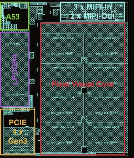
The pixel visual core is designed as a co-processor for various consumer products. Although it's currently only used in the Pixel 2 smartphone, Google have plans to use it in other IoT products in the future. The chip itself incorporates a dedicate ARM Cortex-A53 core which handles the application-level resource requests and configures the core to handle the specific workload. For example, if the application sends a request to capture an image using HDR+, the management core will reconfigure the processing units such that an image captured by the camera will get processed and transformed into HDR+ format. The PVC is optimized for high performance by racing to sleep with a power budget of 6-8 W for very short bursts for around 10-20 seconds an dropping back down to milliwatt when idle. The chip relies equally on both hardware and software in order to achieve the high performance and efficiency by using TensorFlow for machine learning and Halide for image processing.
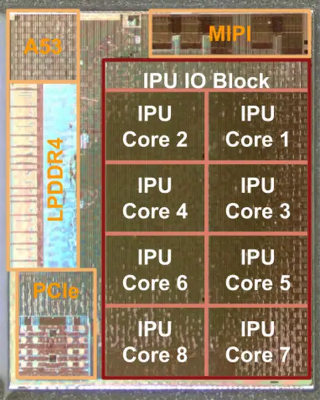
The chip incorporates eight image processing units (IPUs) custom cores, each comprise 512 arithmetic logic units consisting of 256 processing elements (PEs) arranged as a 16 x 16 2-dimensional array. Those cores execute a custom VLIW ISA designed to expose maximum instruction-level and multiple program data parallelism. Though the chip supports 32-bit integers, the native operations are done on a much simpler logic that operates on 8-bit and 16-bit integers, thus larger data sizes will operate at half throughput. The basic primitive of the stencil operations is the multiply-accumulate which can accumulate 32 bits and multiply 16 bits.
Die
Floorplan
Die
- TSMC 28nm 28HPM process
| designer | Google + |
| first announced | October 17, 2017 + |
| first launched | October 17, 2017 + |
| full page name | google/pixel visual core + |
| isa | vISA + and pISA + |
| ldate | October 17, 2017 + |
| manufacturer | TSMC + |
| market segment | Mobile + and Embedded + |
| name | Pixel Visual Core + |
| part number | X726C502 + |
| process | 28 nm (0.028 μm, 2.8e-5 mm) + |
| s-spec | SR3HX + |
| tdp | 8 W (8,000 mW, 0.0107 hp, 0.008 kW) + |
| technology | CMOS + |

