From WikiChip
z14 - Microarchitectures - IBM
| Edit Values | |
| z14 µarch | |
| General Info | |
| Arch Type | CPU |
| Designer | IBM |
| Manufacturer | GlobalFoundries |
| Introduction | July 17, 2017 |
| Process | 14 nm |
| Pipeline | |
| Type | Superscalar, Pipelined |
| Instructions | |
| ISA | z/Architecture |
| Succession | |
z14 was a z/Architecture-based microarchitecture designed by IBM and introduced in 2017 for their z14 processors and mainframes. The z14 microarchitecture replaced the z13.
Contents
Process Technology
z14-based microprocessors are manufactured on GlobalFoundries's 14 nm FinFET Silicon-On-Insulator (SOI).
Architecture
Key changes from z13
- 14 nm process (from 22 nm)
- Higher clock frequency (5.2 GHz from 5 GHz)
- Higher scalability
- Up to 170-way multiprocessing (from 141-way)
- Core
- Improved Operand Store Compare (OSC) prediction
- Faster branch wakeup
- Improved instruction delivery
- Cache
- New directory design
- Power efficient
- L1I$ increased to 128 KiB/core (from 96 KiB/core; 33% increase)
- L2D$ increased to 4 MiB/core (from 2 MiB/core; 100% increase)
- L3$ increased to 128 MiB/CP (from 64 MiB/CP; 100% increase)
- New 672 MiB/drawer of shared L4
- New directory design
- Central Processor Assist for Cryptographic Function (CPACF)
- Dedicated co-processor for each core
- Claims 6x faster encryption functions (vs. z13)
- 4x Advanced Encryption Standard (AES) speedup
- Support for True Random Number Generator
- New support for SHA-3 standard
| This section requires expansion; you can help adding the missing info. |
Overview
| This section is empty; you can help add the missing info by editing this page. |
Die
Core
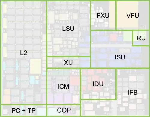
Below is a layout of a single physical core:
- L2 - L2I$ + L2D$
- PC + TP - Core pervasive unit (instrumentation/error collection) + Trap
- LSU - Load-store unit (+ L1D$)
- XU - Translation unit (TLB + DAT)
- ICM - Instruction cache & merge
- COP - Dedicated Co-Processor
- FXU - Fixed-point unit
- VFU - Vector and Floating point Unit
- ISU - Instruction sequence unit
- RU - Recovery unit
- IDU - Instruction decode unit
- IFB - Instruction fetch and branch prediction
Single-chip module (SCM)
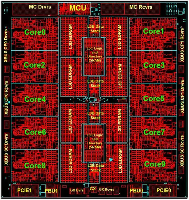
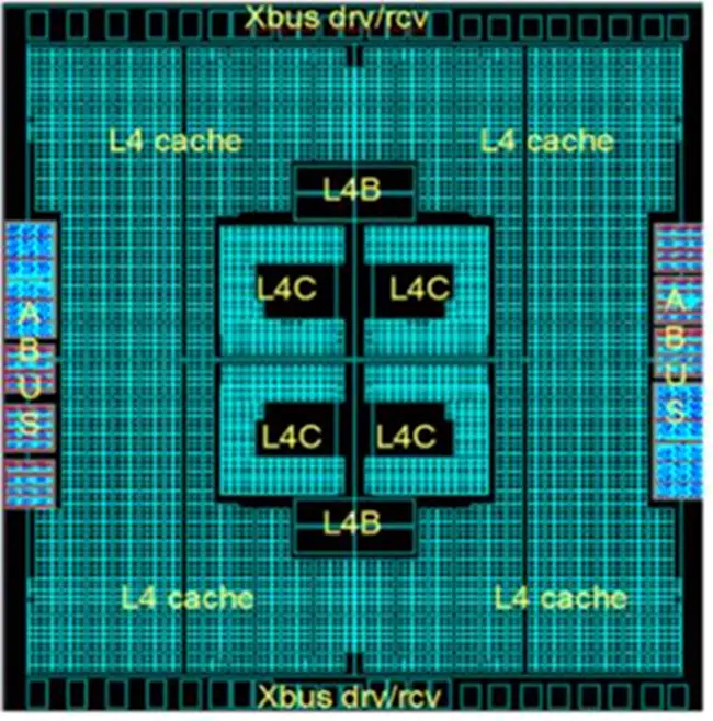
IBM's z14 Single-Chip Module (SCM) consists of a multi-layer metal substrate module that includes either:
- 1x Processor Unit (PU)
- 1x System Controller (SC)
Processor Unit (PU) Chip
- IBM's developed (now GlobalFoundries) 14HP Process
- CMOS FinFET SOI
- 17 Metal Layers
- 25.3 x 27.5 mm die
- 695.75 mm² die size
- deca-core
- 5.2 GHz (192 ps cycle time)
System Controller (SC) Chip
- IBM's developed (now GlobalFoundries) 14HP Process
- CMOS FinFET SOI
- 17 Metal Layers
- 25.3 x 27.5 mm die
- 695.75 mm² die size
- 7,100,000,000 transistors
- + 2,100,000,000 cells of eDRAM (~2.1B xTors + 2.1B capacitors)
- 672 MiB shared eDRAM L4 Cache
Facts about "z14 - Microarchitectures - IBM"
| codename | z14 + |
| designer | IBM + |
| first launched | July 17, 2017 + |
| full page name | ibm/microarchitectures/z14 + |
| instance of | microarchitecture + |
| instruction set architecture | z/Architecture + |
| manufacturer | GlobalFoundries + |
| microarchitecture type | CPU + |
| name | z14 + |
| process | 14 nm (0.014 μm, 1.4e-5 mm) + |


