(→Die size) |
|||
| Line 55: | Line 55: | ||
* 246 mm² (BDW LCC) | * 246 mm² (BDW LCC) | ||
| | | | ||
| − | + | * 2x 74 mm² + 1x 125 mm² (Matisse) | |
| + | * 213 mm² (Pinnacle Ridge) | ||
| + | * 213 mm² (Summit Ridge) | ||
| + | * 210 mm² (Picasso) | ||
| + | * 210 mm² (Raven Ridge) | ||
| + | * 199 mm² (Comet Lake 10C) | ||
| + | * 174 mm² (Coffee Lake 8C) | ||
| + | * 156 mm² (Renoir) | ||
| + | * 150 mm² (Coffee Lake 6C) | ||
| + | * 123 mm² (Ice Lake 4C) | ||
| + | * 122 mm² (Skylake 4C) | ||
| + | * 102 mm² (Skylake 2C) | ||
| | | | ||
* 163 mm² (A5X) | * 163 mm² (A5X) | ||
Revision as of 12:09, 11 May 2020


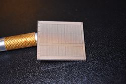
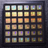
A die is the actual bare IC chip and is the final product of the fabrication process. It is the individual chip made following the singulation of a wafer. Dies typically undergo packaging before being sold to the customer as a final product.
Overview
The die is the final product of the fabrication process. A fully processed wafer will under singulation following probing. Depending on the application, the die may be shipped to an assembly/packaging plant where it will undergo encapsulation, producing the final chip that ships to customers.
Die size
Die size refers to the length and width of the die. Since the die size and shape determines the total number of dies that may be realized from a single wafer, the die size is a strong indicator of cost.
| Select Large Dies | |||
|---|---|---|---|
| GPU | Server | Desktop | Mobile |
|
|
|
|
This list is incomplete; you can help by expanding it.