From WikiChip
Difference between revisions of "amd/microarchitectures/zen 3"
(→Key changes from {{\\|Zen 2}}) |
|||
| Line 45: | Line 45: | ||
* [[7_nm_lithography_process#N7.2B|7 nm+ process]] (from [[7 nm]]) , 20% more density and 10% power reduction compared to Zen 2. EUV (Extreme Ultraviolet) lithography 7nm+. | * [[7_nm_lithography_process#N7.2B|7 nm+ process]] (from [[7 nm]]) , 20% more density and 10% power reduction compared to Zen 2. EUV (Extreme Ultraviolet) lithography 7nm+. | ||
* Decreasing the amount of CCXs per CCD from 2 to 1 | * Decreasing the amount of CCXs per CCD from 2 to 1 | ||
| + | * Decrease memory latency | ||
{{expand list}} | {{expand list}} | ||
Revision as of 16:37, 7 May 2020
| Edit Values | |
| Zen 3 µarch | |
| General Info | |
| Arch Type | CPU |
| Designer | AMD |
| Manufacturer | TSMC |
| Introduction | 2020 |
| Process | 7 nm+ |
| Succession | |
Zen 3 is a planned microarchitecture being developed by AMD as a successor to Zen 2.
Contents
History
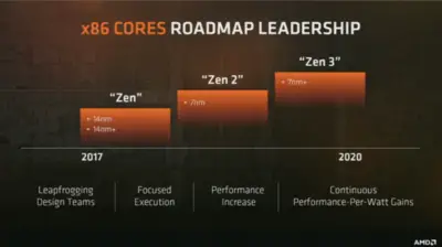
Zen 3 was formally disclosed in a roadmap by Lisa Su, AMD's CEO, during AMD's Tech Day in February of 2017. Zen 3 will be the 3rd iteration of the Zen microarchitecture. On Investor's Day in May 2017 Jim Anderson, AMD Senior Vice President, confirmed that Zen 3 is set to utilize 7nm+ process.
Codenames
| Core | C/T | Target |
|---|---|---|
| Milan | ?/? | High-end server multiprocessors |
| Genesis Peak | ?/? | Workstation & enthusiasts market processors |
| Vermeer | ?/? | Mainstream to high-end desktops & enthusiasts market processors |
| Cezanne | ?/? | Mainstream desktop & mobile processors with GPU |
Process technology
Zen 3 will be fabricated on TSMC's 7nm+ process.
Architecture
Nothing is currently known about the architectural improvements that is being done for Zen 3.
Key changes from Zen 2
- 7 nm+ process (from 7 nm) , 20% more density and 10% power reduction compared to Zen 2. EUV (Extreme Ultraviolet) lithography 7nm+.
- Decreasing the amount of CCXs per CCD from 2 to 1
- Decrease memory latency
This list is incomplete; you can help by expanding it.
References
- AMD 'Tech Day', February 22, 2017
- AMD 2017 Financial Analyst Day, May 16, 2017
See Also
Facts about "Zen 3 - Microarchitectures - AMD"
| codename | Zen 3 + |
| designer | AMD + |
| first launched | 2020 + |
| full page name | amd/microarchitectures/zen 3 + |
| instance of | microarchitecture + |
| manufacturer | TSMC + |
| microarchitecture type | CPU + |
| name | Zen 3 + |

